• Welcome to TechPowerUp Forums, Guest! Please check out our forum guidelines for info related to our community.

Apple M1 & A14 Die Shot Comparison Shows Differences in SoC Design

Joined
Mar 31, 2020
Messages
1,519 (0.79/day)
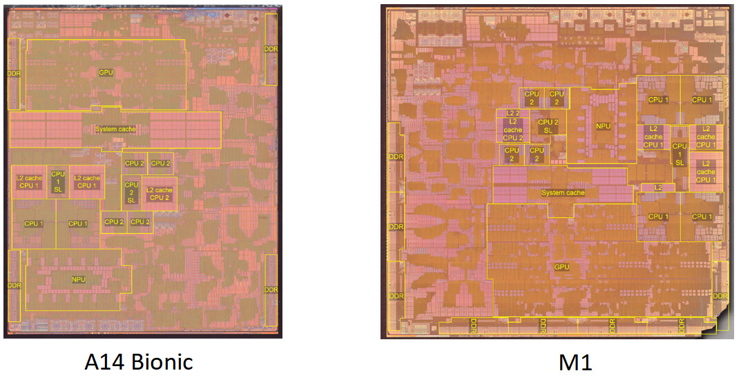
When Apple first announced the M1, questions arose about the differences between it and the A14 chip which both share many architectural features and are both manufactured on TSMC's 5 nm process. Semiconductor analysis firm TechInsights has recently published die photos of the two processors and a summary of the changes.

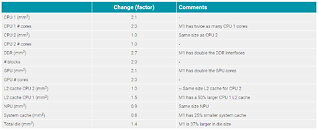
The M1 features four high-performance Firestorm cores and four energy-efficient IceStorm cores for a total of eight CPU cores. The A14 only features six CPU cores with two high-performance Firestorm cores and four energy-efficient IceStorm cores. The M1 includes doubles the amount of GPU cores and DDR interfaces then found on the A14. The M1 also incorporates silicon not found on the A14 including the Apple T2 security processor and other controllers. These additions result in a die size 37% larger than the A14.


View at TechPowerUp Main Site
 
Its amazing to see how much CPU performance these SOC have when so little of the die is dedicated to the CPU.
 
Probably the most interesting stuff here, is that CPUs are just a small part of the whole die.
 
Jumping the gun a little bit. The comparison should be made between the X or Z variants of the A14. You'll find those in the iPads Pro, next year.
 
Jumping the gun a little bit. The comparison should be made between the X or Z variants of the A14. You'll find those in the iPads Pro, next year.

yeah exactly, the question is, is it just an iPad pro chip for the most part? yes, sadly

i wanted an iPad Pro chip with double the GPU for the desktop (and maybe even GDDR6 memory)... or ever 4x the GPU, the GPU is much too slow for something that can't have expansion
 
Its amazing to see how much CPU performance these SOC have when so little of the die is dedicated to the CPU.

It's better actually, as bigger CPU area would mean more delays in signal propagation. Speed of light might be incredibly high to us mortals, but still isn't unlimited. And while working on ns or lesser timescale, is actually relevant.
 
Its amazing to see how much CPU performance these SOC have when so little of the die is dedicated to the CPU.

True, but thinking about it again, I've seen AMD's APU's, the GPU takes so much die area compared to CPU cores and also the uncore area is big. But we know x86 cores are big dies also. Now we see ARM cores which are much smaller and putting these beside the rest (GPU and uncore) gives you an idea of how small ARM cores are.
 
Those diagrams are leaving much to be desired. What's with all the empty unexplained space?
Fixed function hardware of various types. TB3 controller, PCIe, DSP(s), encode/decode blocks, WiFi, modem, etc., etc. Identifying those blocks from a die shot is essentially impossible.

Jumping the gun a little bit. The comparison should be made between the X or Z variants of the A14. You'll find those in the iPads Pro, next year.
I would frankly expect those to run a cut-down version of the M1 - why not, when the silicon works that well? They might call it A14X or some such, but I'd be surprised if they made another piece of silicon given how close to the M1 it will inevitably be.


One question from this (admittedly very high level overview): the big CPU cores look essentially identical. Does this mean that the reported in-silicon optimizations for X86 emulation are also there in the A14 lineup? That would make for some ... interesting possibilities if this hardware wasn't completely locked down. Emulated Windows 10 on an iPhone? :P
 
Die size & performance aside, I find it interesting that a company like Apple, with all it's complexities, expertise, marketing and R&D skills, would stick to such a simple naming scheme for it's processors.... unlike Intel's ungodly clusterf*ck of names of i3-/5-/7-/9-7/8/9/10-xxx-xxx-xxx, and AMD's similar path... :)
 
Its amazing to see how much CPU performance these SOC have when so little of the die is dedicated to the CPU.

This is entirely the other way around, per core these CPUs use way more transistors than the biggest Intel and AMD cores out there.

Probably the most interesting stuff here, is that CPUs are just a small part of the whole die.

They're actually huge, remember that these SoCs are pushing 10 billion+ transistors. Most high end SoCs for phones are no where near that.
 
Die size & performance aside, I find it interesting that a company like Apple, with all it's complexities, expertise, marketing and R&D skills, would stick to such a simple naming scheme for it's processors.... unlike Intel's ungodly clusterf*ck of names of i3-/5-/7-/9-7/8/9/10-xxx-xxx-xxx, and AMD's similar path... :)

Because Apple doesn't sell CPUs so there is no marketing nonsense.
 
DSP’s (Camera processor), PCIe controller, USB, T2 security processor.
Fixed function hardware of various types. TB3 controller, PCIe, DSP(s), encode/decode blocks, WiFi, modem, etc., etc. Identifying those blocks from a die shot is essentially impossible.
Figured it would be those kinds of things, but they really didn't spell it out. It'd be cool to see how all of those types of functional parts are spaced on dies.
 
Figured it would be those kinds of things, but they really didn't spell it out. It'd be cool to see how all of those types of functional parts are spaced on dies.
It would be, but I've never seen them marked out on a die shot, likely because it would then just be a giant blob labeled "fixed function hardware etc." Not much point in that.
 
Because Apple doesn't sell CPUs so there is no marketing nonsense.
Well, to be moar accurate, they do, just not seperately... they still have to convince people (marketing) to buy their 'puters with whatever chips they make for them, which makes the simpler names better for those people who may be somewhat disenchanted with those other naming schemes IMHO :)
 
Its amazing to see how much CPU performance these SOC have when so little of the die is dedicated to the CPU.
I'm guessing you haven't seen many die shots lately. The CPU has ceased to be take more than half the die like a decade ago.
Here's Ivy Bridge, 8 years ago: https://www.anandtech.com/show/5771/the-intel-ivy-bridge-core-i7-3770k-review/3 (I know the CPU space looks bigger than M1's, but you have to consider Ivy Bridge doesn't have as many things integrated)

Die size & performance aside, I find it interesting that a company like Apple, with all it's complexities, expertise, marketing and R&D skills, would stick to such a simple naming scheme for it's processors.... unlike Intel's ungodly clusterf*ck of names of i3-/5-/7-/9-7/8/9/10-xxx-xxx-xxx, and AMD's similar path... :)
For better or worse, Apple has this thing about selling one or two SKUs of everything (there are exceptions). Plus, they don't sell the CPU on its own. A few years down the road, I wouldn't be surprised if they sweep most CPU technical data under the rug and only advertise "Apple 2025 CPU/SoC".
 
Back
Top