• Welcome to TechPowerUp Forums, Guest! Please check out our forum guidelines for info related to our community.
  • The forums have been upgraded with support for dark mode. By default it will follow the setting on your system/browser. You may override it by scrolling to the end of the page and clicking the gears icon.

ASML Finishes Development of EUV Pellicles for Greater Sub-7nm Yields

Raevenlord

News Editor
Joined
Aug 12, 2016
Messages
3,755 (1.15/day)
Location
Portugal
System Name The Ryzening
Processor AMD Ryzen 9 5900X
Motherboard MSI X570 MAG TOMAHAWK
Cooling Lian Li Galahad 360mm AIO
Memory 32 GB G.Skill Trident Z F4-3733 (4x 8 GB)
Video Card(s) Gigabyte RTX 3070 Ti
Storage Boot: Transcend MTE220S 2TB, Kintson A2000 1TB, Seagate Firewolf Pro 14 TB
Display(s) Acer Nitro VG270UP (1440p 144 Hz IPS)
Case Lian Li O11DX Dynamic White
Audio Device(s) iFi Audio Zen DAC
Power Supply Seasonic Focus+ 750 W
Mouse Cooler Master Masterkeys Lite L
Keyboard Cooler Master Masterkeys Lite L
Software Windows 10 x64
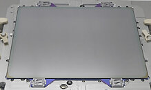
ASML has finally finished development of EUV (Extreme Ultra Violet) pellicles to be employed in manufacturing processes that use the most energetic frequency of visible light to etch semiconductors onto wafers. Pellicles have been used for decades in the industry, and they are basically ultra-thin membranes that protect photomasks during the etching process - impeding particles from depositing in the substrate, which could lead to defects at the wafer level for every subsequent patterning that is laid on top of the impurity. Manufacturers such as TSMC have deployed EUV-powered manufacturing processes, but they have had to toil with potentially lower yields and increased costs with wafer analysis so as to reduce chances of defects appearing.

It's been a long time coming for EUV-capable pellicles, because these have different requirements compared to their traditional, non-EUV counterparts. However, once they are available on the market, it's expected that all semiconductor manufacturers with bleeding-edge manufacturing processes integrate them into their production flows. These will allow for better yields, which in turn should reduce overall pricing for the manufacturing processes. As an example, these EUV masks could be deployed on TSMC's 7 nm, 6 nm, 5 nm, and so on and so on. Other players other than ASML are also finishing their pellicle design, so the industry will have multiple options to integrate into their processes.


View at TechPowerUp Main Site | Source
 
Finally, great news, now we might see everyone doing better yields, this has been badly needed these last two years.
By every foundrie doing cutting edge nodes too.
 
Last edited:
Not gonna help with the current shortages though.
 
a picture says more then a thousand words....unless when it doesn't
 
a picture says more then a thousand words....unless when it doesn't

I deducted that 'thing' must be an EUV Pellicle. (s?)
 
a picture says more then a thousand words....unless when it doesn't
I dont see what you mean. :p :rolleyes:


As wafers get thinner, there will be bigger need for these kinds of developments just to keep moving forward. Still waiting on the nanotube tech to mature.
 
question is: how much EUV light is 'consumed' by these peliciles. EUV light is super expensive to create, and heavily absorbed by any matter, and even air (EUV light path bust be in vaccum, for this reason). Even mirros reflects only 5% EUV light, so they must use special multilayer mirrors with 50 layers, to increase light reflactance to 70%, but this is serious technological challenge.
 
I dont see what you mean. :p :rolleyes:


As wafers get thinner, there will be bigger need for these kinds of developments just to keep moving forward. Still waiting on the nanotube tech to mature.
They have used pellicles for ages, the problem was the type used before, typically for duv ( traditional 248/193nm light sources) deteriorated way to quickly at an unusable rate for higher power and 13nm(Euv) light sources, I don't know if they even used them, but it then also limited euv use to a layer or two on present design's.
And they are not cheap so continued replacement (If used)hit chip costs.
Now less particulate damage, higher yields, more chips.

But 9/12 months until that kicks in on shop shelf's.

That's down to 1Nm(manufacturers speak 3Nm real) fully sorted on traditional lytho afaik.
New tech would obviously be beneficial like GAO or nano ribbons.
 
Last edited:
light is super expensive to create
What what? Please just don't create new flat Earth myth in term that corporations and merchant will use for the next excuse for more expensive prices for components! That is not true!
 
EUV pellicles are not that new. However, this new one lets 90% of light pass through, and this is an important development as it enables a lithography machine to process more wafers per day.

ASML announced months ago that this new type would be available at the end of 2020, and now it's finally here.
 
What what? Please just don't create new flat Earth myth in term that corporations and merchant will use for the next excuse for more expensive prices for components! That is not true!
He isn't wrong the 13nm euv light sources took ages to develop, cost lot's, use two to three times the wattage and Were , possibly not now, dieing quicker.
They are as you should imagine some of the most highly developed, qualified and tuned light sources about , taking quite some effort to make on their own.
Like any other development in this kind hardware. Excuses for uplifting prices for peasants because they don't know that better quality made more usable chips per wafer and this is fully offset by the slightly increased production costs. Because in production of chips this process is just one of many others. Price of chips is not only price of it's production. Just one part of one production process which is completely conpesate at more usable chips per wafer.
 
Like any other development in this kind hardware. Excuses for uplifting prices for peasants because they don't know that better quality made more usable chips per wafer and this is fully offset by the slightly increased production costs. Because in production of chips this process is just one of many others. Price of chips is not only price of it's production. Just one part of one production process which is completely conpesate at more usable chips per wafer.
Look , you can throw vitreal at them all day , they are not excuses.
Why do you think other foundries and machine tool maker's are not about.
The cost of development to be competitive.

As the node scales and yields improve price naturally decreases, Unless the supply is still constrained.
 
a picture says more then a thousand words....unless when it doesn't
If someone said that was an injection molding of an old Acer laptop top cover, it would be believable.
 
Like any other development in this kind hardware. Excuses for uplifting prices for peasants because they don't know that better quality made more usable chips per wafer and this is fully offset by the slightly increased production costs. Because in production of chips this process is just one of many others. Price of chips is not only price of it's production. Just one part of one production process which is completely conpesate at more usable chips per wafer.
Slightly increased production costs? Good one.
Why don't you start your own fab if you can make chips on the cheap?
 
Slightly increased production costs? Good one.
Why don't you start your own fab if you can make chips on the cheap?
The on-duty reference point. This is yours, it's purely political teasing. You know very well that at this stage of development, where there are almost no nanometers left to use, start from scratch and work with an advanced technological process, it is impossible for someone who is not a multi-billionaire. At the same time, the current manufacturers already have the factories built, the technological lines and the necessary finances. As well as the necessary specialists.
 
The on-duty reference point. This is yours, it's purely political teasing. You know very well that at this stage of development, where there are almost no nanometers left to use, start from scratch and work with an advanced technological process, it is impossible for someone who is not a multi-billionaire. At the same time, the current manufacturers already have the factories built, the technological lines and the necessary finances. As well as the necessary specialists.
You couldn't be more wrong. New fabs are almost always built from scratch. And even when retooling happens, you don't retool from 14nm to 10nm. You only retool something "ancient", like 32nm+.
 
The on-duty reference point. This is yours, it's purely political teasing. You know very well that at this stage of development, where there are almost no nanometers left to use, start from scratch and work with an advanced technological process, it is impossible for someone who is not a multi-billionaire. At the same time, the current manufacturers already have the factories built, the technological lines and the necessary finances. As well as the necessary specialists.

Your entire idea falls flat if you take a detailed look at China and how its fabs are getting to smaller nodes. You can't tell anyone they haven't got the billions for it. And still....

Its really very simple, the smallest nodes are the cutting edge, and you can't 'just do that', its similar to projects in space. Everything is new and if its not, its not worth doing, while the margins for error are tiny or non existant altogether.
 
Back
Top