• Welcome to TechPowerUp Forums, Guest! Please check out our forum guidelines for info related to our community.

AMD Files Patent for its Own x86 Hybrid big.LITTLE Processor

btarunr

Editor & Senior Moderator
Staff member
Joined
Oct 9, 2007
Messages
47,684 (7.42/day)
Location
Dublin, Ireland
System Name RBMK-1000
Processor AMD Ryzen 7 5700G
Motherboard Gigabyte B550 AORUS Elite V2
Cooling DeepCool Gammax L240 V2
Memory 2x 16GB DDR4-3200
Video Card(s) Galax RTX 4070 Ti EX
Storage Samsung 990 1TB
Display(s) BenQ 1440p 60 Hz 27-inch
Case Corsair Carbide 100R
Audio Device(s) ASUS SupremeFX S1220A
Power Supply Cooler Master MWE Gold 650W
Mouse ASUS ROG Strix Impact
Keyboard Gamdias Hermes E2
Software Windows 11 Pro
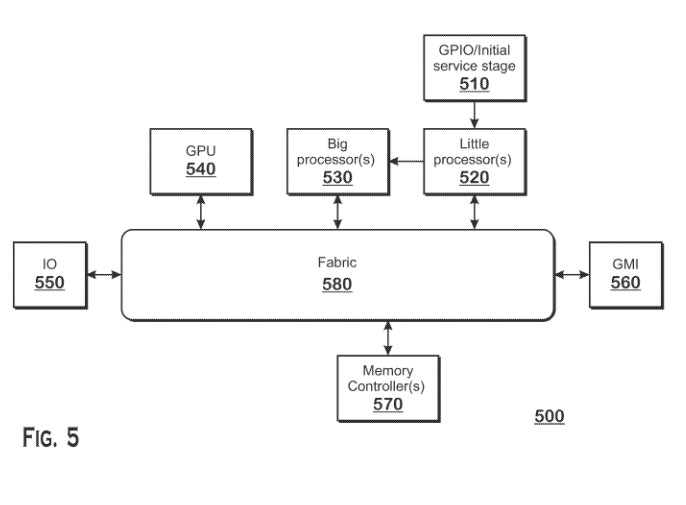
AMD is innovating its own x86 hybrid processor technology formulated along the Arm big.LITTLE hybrid CPU core topology that inspired Hybrid processors by Intel. Under this, the processor has two kinds of CPU cores with very different performance/Watt bands—one kind focuses on performance and remains dormant under mild processing loads; while the other hand handles most lightweight processing loads that don't require powerful cores. This is easier said than done, as the two kinds of cores feature significantly different CPU core microarchitectures, and instruction sets.

AMD has filed a patent describing a method for processing workloads to be switched between the two CPU core types, on the fly. Unlike homogenous CPU core designs where workload from one core is seamlessly picked up by another over a victim cache like the L3, there is some logic involved in handover between the two core types. According to the patent application, in an AMD hybrid processor, the two CPU core types are interfaced over the processor's main switching fabric, and not a victim cache, much in the same way as the CPU cores and integrated GPU are separated in current-gen AMD APUs.


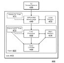
According to the patent application, AMD's CPU core type switching logic is dictated by a number of factors, such as CPU core utilization of the low-power color, its memory utilization, the need for instruction sets only found with the performance core, and machine architecture states. The patent also briefly references a power-management mechanism that saves system power by gating the two core types based on utilization. Power savings are the primary objective of any big.LITTLE topology.

The patent description can be accessed here.

View at TechPowerUp Main Site
 
I wonder why AMD wants to make the big little architecture a thing. They have a noticeable advantage in efficiency.

From the graphs it looks like the big and small core are separated and connected via fabric. So different chiplets? I suppose so.
 
I wonder why AMD wants to make the big little architecture a thing. They have a noticeable advantage in efficiency.

From the graphs it looks like the big and small core are separated and connected via fabric. So different chiplets? I suppose so.
Pic No.1 shows this is an APU design.
They might wanna implement Big.Little architecture to mobile APUs to further enhance power saving capabilities.
 
If they will use it, I hope that will be only laptop processors. Desktop users doesn't need that.

However there is probability that they just need to make patent just to enable using it in future IF some-when it will be needed.
 
I wonder why AMD wants to make the big little architecture a thing. They have a noticeable advantage in efficiency.

From the graphs it looks like the big and small core are separated and connected via fabric. So different chiplets? I suppose so.
Mobile and nextgen consoles can use this. Despite certain advantages, AMD still hasn't picked up in mobile. They cannot fall behind the curve while Intel starts marketing their bigLITTLE implementation as the best thing since sliced bread. AMD cannot gain marketshare by being just a bit better than Intel, thanks to fan boys and subsidy-drunk OEM marketplace.
 
Mobile and nextgen consoles can use this. Despite certain advantages, AMD still hasn't picked up in mobile. They cannot fall behind the curve while Intel starts marketing their bigLITTLE implementation as the best thing since sliced bread. AMD cannot gain marketshare by being just a bit better than Intel, thanks to fan boys and subsidy-drunk OEM marketplace.
By mobile you mean laptops or ULP kinda like tablets? Because AMD certainly have picked up in laptop segment, it's just the wafer crunch which is severely hampering their market share uptick! As for Intel yeah much like ARM, AMD probably also wants to list more cores, even if they're small ones, as a marketing point.
 
Last edited:
Does AMD have a little core in development then? Their AM1 stuff is pretty old.
 
By mobile you mean laptops or ULP kinda like tablets? Because AMD certainly have picked up in in laptop segment, it's just the wafer crunch which is severely hampering their market share uptick! As for Intel yeah much like ARM, AMD probably also wants to list more cores, even if they're small ones, as a marketing point.

I'm including the laptops as well as tablets. AMD is still getting the low-to-mid-tier treatment while top tier models are mostly Intel. There are even examples of AMD models being intentionally crippled: component, material and configuration. Intel is fighting back hard and not only in the R&D and marketing departments, if you know what I mean. That's why AMD can use any advantage they can get, even if it's to tick a marketing box. This is more than just a marketing angle if you ask me. There are many real use cases...

I hope this to be not out in real desktop products. Too copy from Intel.

ARM you mean. Sigh.:rolleyes:
Real (whatever that means) desktop products are only one segment, you know, right? This is very relevant in many environments where power and heat are and will always be bottlenecks...
 
If they will use it, I hope that will be only laptop processors. Desktop users doesn't need that.

However there is probability that they just need to make patent just to enable using it in future IF some-when it will be needed.
I don't agree. For most users, even on desktop, the CPU spends a lot of time in low power scenarios, such as browsing & watching media, where big.little will benefit power draw. Even games are mostly low power scenario's. I have a very power hungry Intel CPU and most games run between 20-60W with a 3060Ti at 1080p. These are places where you can push power draw down with big.little.

Power draw in low usage cases is already a place where AMD is weak and where they draw more power than Intel even when in full load cases they destroy Intel on performance/W so it's a good thing they're trying to improve on this.
 
I hope they keep this stuff away from desktops.
 
I hope they keep this stuff away from desktops.
I kinda see this design could be intended for entry level, low budget stuff. I doubt it could match performance of a full fledged chip.
 
I don't agree. For most users, even on desktop, the CPU spends a lot of time in low power scenarios, such as browsing & watching media, where big.little will benefit power draw. Even games are mostly low power scenario's. I have a very power hungry Intel CPU and most games run between 20-60W with a 3060Ti at 1080p. These are places where you can push power draw down with big.little.

Power draw in low usage cases is already a place where AMD is weak and where they draw more power than Intel even when in full load cases they destroy Intel on performance/W so it's a good thing they're trying to improve on this.
Power draw is one of the thing that can benefits from big-little core but that is not the only one.

Die utilization is another one. smaller simpler core to use way less space versus their relative performance. You can put them more in the same space. Big core are really for the the single threaded load. You could probably get higher performance per die space in highly multithreaded code by using more smaller cores in the same die space. I am not sure about game (altought if the main thread run in the big core, i don't see why it wouldn't be good) but many workload could benefits from it like video encoding, Rendering, etc.

Larger cache might also change how CPU are made, if the L3 always contain what the CPU want to execute, it may no longer need to have all the mechanism there to improve overall performance while the CPU wait for Data.
 
I wonder why AMD wants to make the big little architecture a thing. They have a noticeable advantage in efficiency.

From the graphs it looks like the big and small core are separated and connected via fabric. So different chiplets? I suppose so.
because big little can bring more efficiency benefits. Imagine a 6500U with 8 cores, 4 small, 4 big and 20 hours of battery life, instead of 10 hours, like we get now.
I also don't understand why people are so against this in desktop. People, leave the engineering side of things to the engineers. If, at the end of the day you get better performance, that is what matters.
Another important point mentioned previously is that in the same die space you can get more performance with more smaller cores compared to fewer big cores. Why? Because having a big core with a huge OOO window and making it work efficiently, that is, use as much of those resources that it has is more difficult than maximizing smaller cores.

So in the end, a 16 big cores vs a 8 big cores and 16 smaller ones might bring you more performance from the 8+16 with similar die space usage, pluuus, you are more efficient when idle/partially loaded thanks to those smaller cores.
 
So in the end, a 16 big cores vs a 8 big cores and 16 smaller ones might bring you more performance from the 8+16 with similar die space usage, pluuus, you are more efficient when idle/partially loaded thanks to those smaller cores.
Yeah, die utilization is a big thing, to add in, for Intel, apparently one of their big cores(Golden Cove) uses as much space as 4(!!!!) little cores(Gracemont). So it would be a scenario of 16 big cores vs 8+32 cores.

I actually think that power efficiency in desktop is also an objective for Intel, for the same reason why they want ATX12VO, power regulations from states/government.
Indeed

Well People talk a lot about IPC, but work accomplish per joule is still a critical point on all platform including desktop. Nobody want to have to deal with a 1000w CPU.

"Little" core aren't only smaller, they use less power for the same amount of work. This means you can do more work with the same power envelope. In the end, this is what everyone want on all platform.
 
How I see it is bigLITTLE approach could be used to vary the L1/L2 cache between dies, vary the core count, and vary the instruction sets. I could see Intel/AMD actually doing per core design changes within a actual chip die. The more multi-core these become the more AMD/Intel will probably want to leverage specific tailored advantages within the cores similar to what AMD did with RNDA to RNDA2 to eek out more performance and efficiency of the design structure. If you have a 8c or 16c chip die half or a quarter of it might have subtle differences to the L1/L2 cache, instruction sets, ect down the road.

A lot of the low hanging fruit from multi-core multi die CPU designs might run it's course a bit so less emphasis on too much general purpose might be the way forward in favor of task specific speeds ups to more latency sensitive workloads that are only lightly threaded for example.

I just see a doorway to dynamic L1/L2 cache size and design structure between chip dies to be leveraged. Why wouldn't you want a L1 or L2 cache that's a bit lower latency than one on another die? Why might you want a bit higher L1/L2 cache latency rather than a cache hit penalty at the same time by accessing the next level cache? There are obvious performance and power efficiency reasons to why cache's are designed a particular way. It's just not possible for them to be perfect across all use cases in terms of performance and efficiency however there is always a balance. I see this is a nice way of achieving higher balance. I do think the L3 cache could absolutely be shared and tasks across the L3 cache combined in highly parallel workloads. Lighter less parallel workloads I could see a round robin cache approach based on the chip die where a task retroactively selects the best suited L1/L2 cache design structure on the fly where it will use one over another to speed up a given part of a given task on hand.
 
Last edited:
AMD has a few potential options here:

Make a new cut-down Zen optimized for die space and low power.

Bring back AMD's Atom competitor with significant updates.

Use ARM cores.

Using ARM cores has been my thought for some time, MS has the ability to do so, the Linux people surely have as well, plus AMD have produced their own ARM CPU's before, so already have some experience with ARM and possibly the most significant point here (apart from the software) is that AMD and Samsung are already collaborating with Samsung Fabricating AMD parts and Samsung licencing AMD RDNA GPU cores for Samsung mobile chips.
 
AMD should just take a chip like the 3300X shrink it to 5nm and then make two other variations on it and combine 3 of those chips on the same substrate. The variations would alter the L1 and L2 cache data width and instruction set sizes and designs slightly and inverted while the 3300X shrunk down to 5nm could remain right in between. Basically they could have 3 different L1 cache designs every L1 cache clock cycle to pick and choose the most optimal option to avoid a cache hit miss penalty and requiring the L2 cache access and same goes for the L2 cache as well to avoid a cache hit miss penalty and accessing the slower in turn L3 cache. It's pretty clear to me the cache structure of different dies and the instruction sets on them are ways to increase IPC and avoid cache hit miss penalties. The L3 cache obviously could be shared while the other parts of the cache differentiated more. I feel that is the way to approach big.LITTLE and down the road it could done more on a per core level or per core cluster level within a chip die similar to how GPU's hand some parts of the design like how RDNA 1 to RDNA2 evolved.
 
AMD has a few potential options here:

Make a new cut-down Zen optimized for die space and low power.

Bring back AMD's Atom competitor with significant updates.

Use ARM cores.

Using ARM cores has been my thought for some time, MS has the ability to do so, the Linux people surely have as well, plus AMD have produced their own ARM CPU's before, so already have some experience with ARM and possibly the most significant point here (apart from the software) is that AMD and Samsung are already collaborating with Samsung Fabricating AMD parts and Samsung licencing AMD RDNA GPU cores for Samsung mobile chips.
It's true that you have windows and Linux version running on ARM. But that do not means it would make sense to use ARM core for the little core. You can't execute x64 code with arm64 code.

The rumors are they would use Zen4 core as the little core and Zen5+ as the big core, all x64.
 
It's true that you have windows and Linux version running on ARM. But that do not means it would make sense to use ARM core for the little core. You can't execute x64 code with arm64 code.
The entire code base would have to be different, not just the 64-Bit stuff, however my line of thinking here is that the "little" cores are there for background tasks and things that simply do not need blazing performance.

MicroShaft and Linux already run the OS and Apps on ARM cores, I see no (good) reason why the OS in either case could not be literally run on top of each other. I would run the "base" OS on the Arm cores so that the base system will natively run low power and background system tasks, with the "upper" OS running the big AMD64 (x86) cores for things that need it.

Arm cores have been heavily optimised for Web Apps and video already, the relatively small performance loss of running Web Apps (browsers primarily) on the "little" Arm cores would likely be unnoticeable except on benchmarks, and Browsers are the only "low power" App that I am aware of that is deceptively needy of high performance CPU's.

On the MS side, there would undoubtedly be a massive cludge, but as Gaming and other high performance needing Apps are slowly moving away from MS to Linux anyway, I would expect Linux to be the ideal OS platform, or I should say, Dual OS platform. There is also no real reason why using such an Arm/AMD64 hybrid CPU cannot be done using Linux on the Arm coses as the "base" OS and Windows on top of that, in many respects this would be the ideal solution.

There would potentially be great boons for system security by going this route of essentially running two OS's one on top of the other, which is commonplace with Servers.

There is still a long time to wait for this to happen, so we will likely not get anything concrete for a couple of years, up until then, this is pure speculation and a thought experiment.

You can't execute x64 code with arm64 code.

Intel's upcoming solution has a similar couple of problems itself, the first is likely not a real issue at all and that is that the "small cores" do not have Hyper Threading, the second issue is that the "small cores" cannot execute AVX512. AVX512 is still not commonly used, and when it is it is typically used in high performance Apps anyway.

Seeing how Intel / MicroShaft / Linux gets round these issues will be interesting as will be the whole operation of the scheduler. From what I have heard, MS has/is putting a lot of effort into this (with Intel) and could give us clues as to how AMD goes about this.

Interesting times ahead, especially for those who will want to use (or just test) how Alder Lake performs on W10 vs W11, and whether MS / Intel make Rocket Lake's big.LITTLE CPU's work properly at all on W10, we shall find out in a few months.
 
Last edited:
Back
Top