• Welcome to TechPowerUp Forums, Guest! Please check out our forum guidelines for info related to our community.

AMD Ryzen Embedded V3000 SoCs Based on 6nm Node, Zen 3 Microarchitecture

btarunr

Editor & Senior Moderator
Staff member
Joined
Oct 9, 2007
Messages
47,670 (7.43/day)
Location
Dublin, Ireland
System Name RBMK-1000
Processor AMD Ryzen 7 5700G
Motherboard Gigabyte B550 AORUS Elite V2
Cooling DeepCool Gammax L240 V2
Memory 2x 16GB DDR4-3200
Video Card(s) Galax RTX 4070 Ti EX
Storage Samsung 990 1TB
Display(s) BenQ 1440p 60 Hz 27-inch
Case Corsair Carbide 100R
Audio Device(s) ASUS SupremeFX S1220A
Power Supply Cooler Master MWE Gold 650W
Mouse ASUS ROG Strix Impact
Keyboard Gamdias Hermes E2
Software Windows 11 Pro
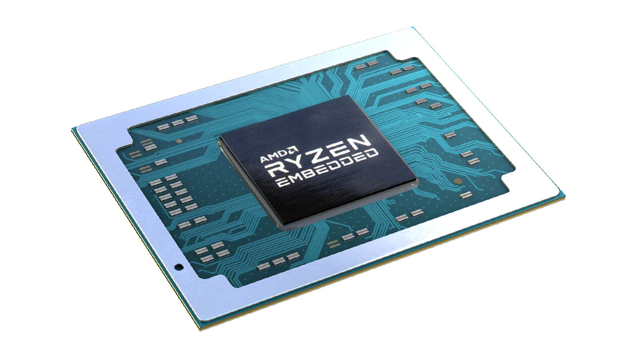
AMD's next generation Ryzen Embedded V3000 system-on-chips aren't simply "Cezanne" dies sitting on BGA packages, but rather based on a brand new silicon, according to Patrick Schur, a reliable source with leaks. The die will be built on the more advanced 6 nm silicon fabrication node, whilst still being based on the current "Zen 3" microarchitecture. There are several things that set it apart from the APU silicon of the current-generation, making it more relevant for the applications the Ryzen Embedded processor family is originally built for.

Built in the FP7r2 BGA package, the V3000 silicon features an 8-core/16-thread CPU based on the "Zen 3" microarchitecture. There are also an integrated GPU based on the RDNA2 graphics architecture, with up to 12 CUs, a dual-channel DDR5 memory interface, a 20-lane PCI-Express 4.0 root complex, with up to 8 lanes put out for PEG; two USB4 ports, and two 10 GbE PHYs. AMD could design at least three SKUs based on this silicon, spanning TDP bands of 15-30 W and 35-54 W.


View at TechPowerUp Main Site
 
So Zen 3, RDNA 2, PCIe 4.0, USB 4, and dual channel DDR5? That's kinda like the perfect version of the current Ryzen mobile chips.
 
Can we get this on laptops too please? lol
 
With 2 Dimm in dual(2x2x32) channels running at 6400MT, that is 102 GB/s of bandwidth. Zen3 8 core already perform well with half that bandwidth so that leave more than enough to the GPU. GPU won't bother of any increased latency the memory would give as they are already build to hide it.

That would be more bandwidth than a Geforce 1030. This should be good enough for light 1080 gaming and medium detail, if not more since RDNA2 GPU is more modern than Pascal. There are no rumours of Infinity cache, but still, RDNA2 could have more L1 and L2 depending on the final layout.


Can't wait to see the final bench. the desktop 5600G and 5700G already have impressive performance (for integrated graphic) with Vega and DDR4. This could be a game changer.
 
It's hardly possible to buy a V2000 board still
 
Hm, that is definitely interesting. Hope most of this (except for the 10G PHYs I guess) carries over to next-gen mobile and desktop APUs. Would make for some very, very compelling products.
 
Can we get this on laptops too please? lol
That will be Rembrandt in laptops, I think.
With 2 Dimm in dual(2x2x32) channels running at 6400MT, that is 102 GB/s of bandwidth. Zen3 8 core already perform well with half that bandwidth so that leave more than enough to the GPU. GPU won't bother of any increased latency the memory would give as they are already build to hide it.
Would still be lower latency than GDDR, which can be a small benefit, though bandwidth is more important.
That would be more bandwidth than a Geforce 1030. This should be good enough for light 1080 gaming and medium detail, if not more since RDNA2 GPU is more modern than Pascal. There are no rumours of Infinity cache, but still, RDNA2 could have more L1 and L2 depending on the final layout.
RDNA1 adds a nee level of cache, a L1 that's shared in the Shader Arrays(10 CUs in 5700xt). This is kept the same in RDNA 2. The old L1 in Vega/GCN is now just L0.

For Rembrandt it appears like they are doing 2 Shaders Arrays of 6 CUs each(3 DCUs) and 2mb of L2, an increase of the 1mb in the Vega iGPUs. So a decent increase in the caches.

Nothing too big of a change though.

Would be really impressive if they could do like Apple and do a shared cache with CPU and iGPU( aka SLC/System level cache for Apple, though other blocks like neural stuff also use it), even more so if they do it with their vertical cache. It would be completely revolutionary in the mobile and integrated gpu space.
But that's just a pipe dream.
That's what a mobile Infinity Cache would likely be, no? A large dedicated cache doesn't make much sense for a mobile iGPU considering die space costs, but if the CPU (and other blocks) could also share it? That would be easier to defend. There's a big question of size though, as even a 16MB cache would take up significant die area.

I don't think we're likely to see stacked cache in mobile yet though. That would necessitate a huge amount of "structural silicon" (i.e. spacers around the cache die) considering the size of APUs compared to a CCX, and would no doubt have some detrimental effects for already thermally constrained mobile designs.
 
That's what a mobile Infinity Cache would likely be, no?
Maybe, it could just be a smaller L3 exclusive to the iGPU. Navi 24 is rumoured to have 16 mb of infinity cache, so a small 8 mb for an iGPU would be pretty helpful already.

AA large dedicated cache doesn't make much sense for a mobile iGPU considering die space costs, but if the CPU (and other blocks) could also share it? That would be easier to defend. There's a big question of size though, as even a 16MB cache would take up significant die area.
It all depends on the node, type of SRAM choosen as well as AMD desire. If you look at Apple(again), you will see that they are a shit ton of cache. 16 mb SLC(system level cache, basically a system wide L3), 16 mb of L2(12 for performance and 4 for efficiency cores) and even enormous L1 caches(320kb for performance and 192kb for efficiency cores).

So, I think that AMD could easily add something like 8 mb as infinity cache. Yes, Apple is in 5nm, but SRAM doesn't scale as logic does, in addition they are going to 6nm anyway(and have a bigger die than Cezanne despite increased density).
I don't think we're likely to see stacked cache in mobile yet though. That would necessitate a huge amount of "structural silicon" (i.e. spacers around the cache die) considering the size of APUs compared to a CCX, and would no doubt have some detrimental effects for already thermally constrained mobile designs.
Probably not since they grind those dies so that they end up with the same height, plus structural silicon might even help with spreading more of the heat.

In addition, could actually reduce power consumption as the part which consumes the most is the data transmission, while processing it is cheap. If you remember Broadwell, it was pretty good in energy consumption and it could even do stuff like turn off under some circumstances.

This would really help with mobile skus. But honestly, I doubt that AMD will do it in the next 2-3 years.
 
Back
Top