• Welcome to TechPowerUp Forums, Guest! Please check out our forum guidelines for info related to our community.

AMD 4700S Desktop Kit Features PlayStation 5 SoC Without iGPU

AleksandarK

News Editor
Staff member
Joined
Aug 19, 2017
Messages
2,999 (1.07/day)
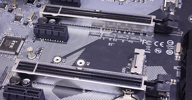
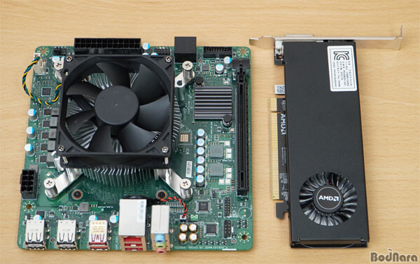
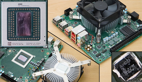
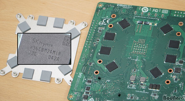
Previously, we have assumed that AMD 4700S desktop kit is based on Xbox Series X APU. Today, according to the findings of Bodnara, who managed to access one of these units, and we got some interesting discoveries. The chip powering the system is actually the PlayStation 5 SoC, which features AMD Zen 2 based system architecture, with 8 cores and 16 threads that can boost up to 3.2 GHz. The board that was tested features SK Hynix GDDR6 memory running at 14 Gbps, placed on the backside of the board. The APU is attached to AMD A77E Fusion Controller Hub (FCH), which was the one powering Xbox One "Durango" SoC, leading us to previously believe that the AMD 4700S is derived from an Xbox Series X system.

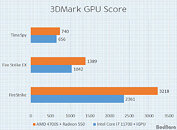
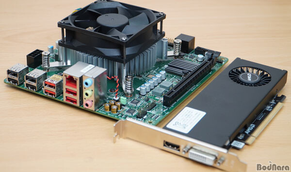
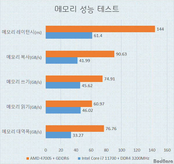
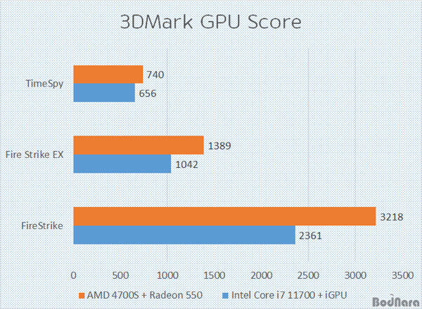
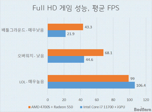
The graphics of this APU are disabled, however, it was the same variant of RDNA 2 GPU used by the PlayStation 5. Right out of the box, the system is equipped with a discrete GPU coming in a form of the Radeon 550, and this configuration was tested by the Bodnara team. You can find the images of the system and some performance results below.
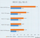
Performance:


View at TechPowerUp Main Site
 
Oh goody, the final specs on the useless box!

I'm curious how that ram performs vs DDR4/5 however
 
I would think the APU is more likely lasered off because it is broken.
 
I would think the APU is more likely lasered off because it is broken.
Either that, or forced to by contract

Like maybe there was a huge order for dev kits that got cancelled and they thought to sell the whole lot off, but had to nerf the GPU first?
The second slot only runs at x4, which would have been for an NVME slot in the console
 
Oh goody, the final specs on the useless box!

I'm curious how that ram performs vs DDR4/5 however
That's the first attached image. The sourced review linked didn't say what software is used and I cant read Korean in the image, nor translate the image (I probably can but don't really want to). The latency and speed seems about right for DDR4, I'm guessing from the top it is latency, write, read and copy. Last row I have no idea). The original review is pretty poor too and reads like an advertisement for the kit. Zero actual CPU bench, some game fps with low requirement games for modern CPU (league, overwatch) and probably GPU bounded "battleground" (translated) which might be PUBG, and didn't go into details at all.
 
Ahhh that LP card is so cute :)
 
The actual bandwidth when using with iGPU would be much higher.
 
I'm definitely not super salty we cant see what the APU would really be like with windows benchmarks for a true comparison to the consoles, nope not at alllllll
 
Given this is a "salvaged parts being sold for cheap" is that a full-fat RX 550 or some bastardised 2GB DDR4 variant?

Even the full-fat RX550 was a lame duck with performance close to the GT1030 but twice the power draw and lacking an encoder to match NVENC. At this performance level, power consumption and encoder performance are kind of a big deal because the actual 3D compute/gaming performance is bad enough to not be worth consdering over an IGP (unless, of course, you don't even HAVE and IGP like in this case).
 
How sick would it be if the CUs actually worked.... If it did, this thing would be used for epic SFF builds
 
I'm definitely not super salty we cant see what the APU would really be like with windows benchmarks for a true comparison to the consoles, nope not at alllllll
The APU with GDDR6 instead of DDR4 would have been really impressive, for sure - 36CUs to the 6700XT's 40CUs but with a more restrictive TDP and having to share the GDDR6 with the CPU cores it would probably still perform exceptionally well. I would have to guess that the power/clock/cache deficit would put it in the ballpark of the rumoured RX 6600 with 28CU. Not bad for something that could rival a NUC.
 
The APU with GDDR6 instead of DDR4 would have been really impressive, for sure - 36CUs to the 6700XT's 40CUs but with a more restrictive TDP and having to share the GDDR6 with the CPU cores it would probably still perform exceptionally well. I would have to guess that the power/clock/cache deficit would put it in the ballpark of the rumoured RX 6600 with 28CU. Not bad for something that could rival a NUC.
Just... that in a gaming laptop. Just do it already AMD. Make a (soldered) DDR6 16GB and 32GB version and have a pro gamer laptop with the same specs as the consoles.

I know how powerful my 5800x can be in a 95W TDP, so i can only dream of what would be possible with laptop optimised parts
 
original ZEN2 is ~~74 mm²
this 4700S ps5 ZEN2 ~~38.5mm² is ~heavily dawngraded to 128 bit though, if it has any impact on games that should be it.

What they should do is integrate 45W ZEN3 shrinked 30mm² on 5nm ondie RX6900~~RTX3090 shrinked to 200mm² and a fast NVMe on the back side.
and call it a day or a ps6 pro. cant wait for the PS6pro.
 
I'd be curious to see how much performance the PCIE 2.0 x4 lane bottleneck higher end discrete GPU's given the higher GDDR6 bandwidth would balance out before the upside of the GDDR6 is outweighed by the higher bus bandwidth of PCIE 3.0 at x4/x8/x16 against a similar Zen 2 CPU and clock frequency. The results would be intriguing and give a good idea of how integrating a single chip of GDDR6 or HBM on MB's might bolster performance used as a cache buffer perhaps. On the note of integrating a single chip of GDDR6 is enough to meet Windows 10 requirements.
 
I would think the APU is more likely lasered off because it is broken.
I would think it is because drivers won't support it (even if the majority of CUs work) and they don't want people mucking around with it regardless and maybe figuring out how to hack the PS5 GPU; Sony may want to keep it to itself for now.
 
Meh

Missing the most important component..............................the igpu.............................
 
Given this is a "salvaged parts being sold for cheap" is that a full-fat RX 550 or some bastardised 2GB DDR4 variant?

Even the full-fat RX550 was a lame duck with performance close to the GT1030 but twice the power draw and lacking an encoder to match NVENC. At this performance level, power consumption and encoder performance are kind of a big deal because the actual 3D compute/gaming performance is bad enough to not be worth consdering over an IGP (unless, of course, you don't even HAVE and IGP like in this case).
RX 550 is faster than GT 1030 GDDR5 and defenitly faster then the DD4 version. And GT 1030 also lacks NVENC. So why spread lie.
 
RX 550 is faster than GT 1030 GDDR5 and defenitly faster then the DD4 version. And GT 1030 also lacks NVENC. So why spread lie.
The RX550 is approximately 6% faster than the GT1030. I said 'performance close to' not 'slower than' so I don't consider that as spreading lies.
GT1030 lacks the Turing NVENC, but I thought it had the older generation Pascal NVENC? I wouldn't know because the 1030 is a turd that I've never purchased; Happy to stand corrected if I'm wrong.

Edit:
Just looked it up, 1050 is the first Pascal card with NVENC, I think I was mis-remembering the controversy surrounding the 1650 getting short-changed on the previous-gen NVENC.
 
Last edited:
original ZEN2 is ~~74 mm²
this 4700S ps5 ZEN2 ~~38.5mm² is ~heavily dawngraded to 128 bit though, if it has any impact on games that should be it.
That's likely mostly due to the cache, the big ass L3 occupies most of the zen 2 die space and they cut it to a fourth(2x4mb vs 2x16mb) for consoles. There's also likely some other space savings as well like shorter pipelines or such since those CPUs don't need to go to more than 3.6/3.8GHz while the desktop parts are made with higher turbo in consideration.
What they should do is integrate 45W ZEN3 shrinked 30mm² on 5nm ondie RX6900~~RTX3090 shrinked to 200mm² and a fast NVMe on the back side.
and call it a day or a ps6 pro. cant wait for the PS6pro.
SRAM caches don't scale that well on nodes. So no, there's never really going to be 30mm2 Zen3 in 5nm.
 
This just... sounds wrong.
iSoC, where the i stands for incomplete
It's less of a mouthful than SoCmGPUfclr (SoC missing GPU for complex licensing reasons)
 
Either that, or forced to by contract
There's another reason: lower TDP and a cheaper VRM. Still, in all probability, AMD could have disabled all the parts that contain any MS's ""intelectual" "property""*, so at least a primitive iGPU would have remained alive, for emergency use. They'd have to include a video output connector, though.

* Intellectual is put in quotes, property is put in quotes, then the whole phrase is put in quotes once again.
 
I'd be curious to see how much performance the PCIE 2.0 x4 lane bottleneck higher end discrete GPU's given the higher GDDR6 bandwidth would balance out before the upside of the GDDR6 is outweighed by the higher bus bandwidth of PCIE 3.0 at x4/x8/x16 against a similar Zen 2 CPU and clock frequency. The results would be intriguing and give a good idea of how integrating a single chip of GDDR6 or HBM on MB's might bolster performance used as a cache buffer perhaps. On the note of integrating a single chip of GDDR6 is enough to meet Windows 10 requirements.


There's however a high latency penalty by using GDDR6 vs DDR4.

Furthermore: it would be cool if the thing could be reverse engineered and perhaps a HDMI output soldered on + working VGA.
 
Back
Top