• Welcome to TechPowerUp Forums, Guest! Please check out our forum guidelines for info related to our community.

AMD "Zen 3" 3D Vertical Cache Detailed Some More

btarunr

Editor & Senior Moderator
Staff member
Joined
Oct 9, 2007
Messages
47,888 (7.38/day)
Location
Dublin, Ireland
System Name RBMK-1000
Processor AMD Ryzen 7 5700G
Motherboard Gigabyte B550 AORUS Elite V2
Cooling DeepCool Gammax L240 V2
Memory 2x 16GB DDR4-3200
Video Card(s) Galax RTX 4070 Ti EX
Storage Samsung 990 1TB
Display(s) BenQ 1440p 60 Hz 27-inch
Case Corsair Carbide 100R
Audio Device(s) ASUS SupremeFX S1220A
Power Supply Cooler Master MWE Gold 650W
Mouse ASUS ROG Strix Impact
Keyboard Gamdias Hermes E2
Software Windows 11 Pro
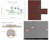
Senior Technology Fellow Yuzo Fukuzaki shed light on the elusive new CPU technology AMD unveiled at its Computex 2021 keynote, 3D Vertical Cache (3DV Cache). The company had then detailed it as an additional 64 MB last-level cache stacked on top of a CCD (CPU core complex die), which significantly improves performance, including a claimed 15% average gain in gaming performance, which accounts for a generational performance gain over "Zen 3." The prototype AMD unveiled in its keynote was based on a Socket AM4 processor with "Zen 3" CCDs that have the 3DV Cache components in place. With two such CCDs, a 16-core processor would end up with 192 MB of L3 cache.

Yuzo Fukuzaki's theory sheds light on the most plausible position of 3DV Cache in the processor's cache hierarchy. Apparently, it expands the CCD's L3 cache, and doesn't serve as an "L4" victim cache to the L3. This way, the cache setup remains transparent to the OS, which sees it as a contiguous 96 MB block of L3 cache (per CCD). The 3DV Cache die is an SRAM chip fabricated on the same 7 nm process as the "Zen 3" CCD. It measures 6 mm x 6 mm (36 mm²), and is located above the region of the CCD that typically has the 32 MB L3 SRAM. Fukuzaki estimates that roughly 23,000 TSVs (through-silicon vias), each about 17 µm in size, connect the 3DV Cache die to the main CCD.


View at TechPowerUp Main Site
 
I am still skeptical of how well this can be cooled, in areas where there is an overlap with the L1 caches for example there is going to be a massive concertation of heat.
 
I wonder if AMD will bring those CPUs to AM4 and especially to older motherboards, like X470 and B450.

On the other hand, next gen APUs, with Zen 4 cores, RDNA1/2 iGPUs, infinity cache and 3D cache, could make today's APUs look like old and very slow trash. Like comparing an AM4 APU with an FM2+ APU.
 
article said:
Apparently, it expands the CCD's L3 cache, and doesn't serve as an "L4" victim cache to the L3. This way, the cache setup remains transparent to the OS, which sees it as a contiguous 96 MB block of L3 cache (per CCD).
Actually, the software doesn't "see" the cache at all, it's completely transparent. What software sees is memory, and thanks to caching this memory is sometimes faster.


I am still skeptical of how well this can be cooled, in areas where there is an overlap with the L1 caches for example there is going to be a massive concertation of heat.
L3 cache doesn't add much heat, and this extra layer will probably act as a heat spreader and will be good enough, unless you're thinking about extreme overclocking.

I'm much more concerned about cost and availability, the latter of which has been a huge limitation for AMD lately.
 
Last edited:
I wonder how AMD will position Zen 4 against this as perfomance seems like will be pretty close, with quite a few workloads possibly being better due to more cache. Maybe this means that the top Zen 4 SKUs will have 3D cache as well?

With that said, I think that pricing is going to be really bad for those Zen3D parts and only for 5900X and 5950X, any lower and it kinda stops making sense.

One random thought that I had was what if AMD plan is to remove L3 cache altogether from the CCD and only have it from the cache die. That could be good for yields as reduces the CCD die considerably(a cache die would also likely be defect resistant since SRAM is easily redundant and thus possibly cheap), though It depends on how costly the 3D packaging is and others factors that I am probably unaware of that could make this unviable. For temperatures, maybe use some of those new 3D packaging tech that allows you to put logic on top. Could also use this as a bridge between CCDs like in the RDNA3 rumours?

That's just a random thought of mine though and probably completely wrong, so just ignore it.
 
I am still skeptical of how well this can be cooled, in areas where there is an overlap with the L1 caches for example there is going to be a massive concertation of heat.
Vcache sits on top of existing one. Cache is not's what causing the heat. The chiplet part that generates heat will be covered by epoxy resin most likely to have it level with vcache.
 
Hmm, this cache isn't 3D and isn't vertical. This is just another but fat layer.
STVs and it is vertical, directly above the existing chip.

Did you expect a skyscraper?

I mean at 7nm it probably scales like a skyscraper.

Cache is the new performance booster, Infonity cache, 3DV cache, the M1.
 
Hmm, this cache isn't 3D and isn't vertical. This is just another but fat layer.
Looks pretty vertical to me:

1628255292809.png
 
I doubt this will help in normal work loads vs alder lake
lol why am I not surprised you are the only person in this thread to come in here talking about intel?

What are you worried about?
 
2TB/s. Bandwidth wise, latency is ten time higher, this is L1 ballpark.
 
STVs and it is vertical, directly above the existing chip.

Did you expect a skyscraper?

I mean at 7nm it probably scales like a skyscraper.

Cache is the new performance booster, Infonity cache, 3DV cache, the M1.
Vertical=90° angle in relation to horizontal, yes!?
 
STVs and it is vertical, directly above the existing chip.

Did you expect a skyscraper?

I mean at 7nm it probably scales like a skyscraper.

Cache is the new performance booster, Infonity cache, 3DV cache, the M1.
That guy comment was pretty rude, but it's not full 3D but more 2.5D

3D chip is not there yet and not around the corner (if it ever come). Right now it's each die are in 2D. they can stack those and have TSV, but it remain that each layer is 2D. 3D will allow very complex transistor layout. It would help with propagation as you would be able to make denser logic with less space. But I am still not even sure we can make those in labs...


Anyway, that do not mean that this 3D cache isn't impressive. It's actually very impressive and only the beginning of die stacking. The next decade will be very interesting, trust me on that. This is only the beginning.
 
I doubt this will help in normal work loads vs alder lake
There should be no doubt that this will help performance, the question is by how much, and in which workloads.

L3 is a spillover cache for L2. Boosting L3 cache will help reduce cache misses, but probably mostly cache lines with instructions, as discarded data cache lines are less likely to be reused quickly, which means the gains will be very workload dependent. But regardless this is a very expensive way to add a little performance. This makes me wonder if this will be reserved for a small selection of premium models.
 
I wonder if they are trying to do with the CPU with what they did to the GPU with the large L3 "infinity" cache??
 
With reports already claiming that Zen4 IPC increase is in the 25%+ area (including an article by this very website that stated 29%) it makes me wonder in the top models of zen4 perhaps 6900x and 6950x, but maybe even the 6800x might also come with this V-cache as well and be something really impressive, like 35%+ core for core performance increase over Zen3?
 
I am still skeptical of how well this can be cooled, in areas where there is an overlap with the L1 caches for example there is going to be a massive concertation of heat.
It will certainly run hotter. The question is whether the IPC gains will make up for the increased heat generated.
 
It will certainly run hotter. The question is whether the IPC gains will make up for the increased heat generated.
95W part CCX L2 cache is about 8.1W in total, according to AMD power map. No, not insignificant, but the surface is also very big, it's about half the size of each CCX. Each core has about the same power draw, but is 30x smaller in size.

Cooling is not an issue.

Source: AMD NDA docs.
 
95W part CCX L2 cache is about 8.1W in total, according to AMD power map. No, not insignificant, but the surface is also very big, it's about half the size of each CCX. Each core has about the same power draw, but is 30x smaller in size.

Cooling is not an issue.

Source: AMD NDA docs.
They're not talking about increased power, the problem could be the greater thickness. You're adding a thick layer of silicon over the main core die: this layer could reduce heat transfer to the IHS, then to the cooler.

But Amd said that:

 
Last edited:
Back
Top