• Welcome to TechPowerUp Forums, Guest! Please check out our forum guidelines for info related to our community.

AMD Ryzen 5 5600G APU Die Shots Published

Joined
Mar 31, 2020
Messages
1,519 (0.82/day)
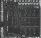
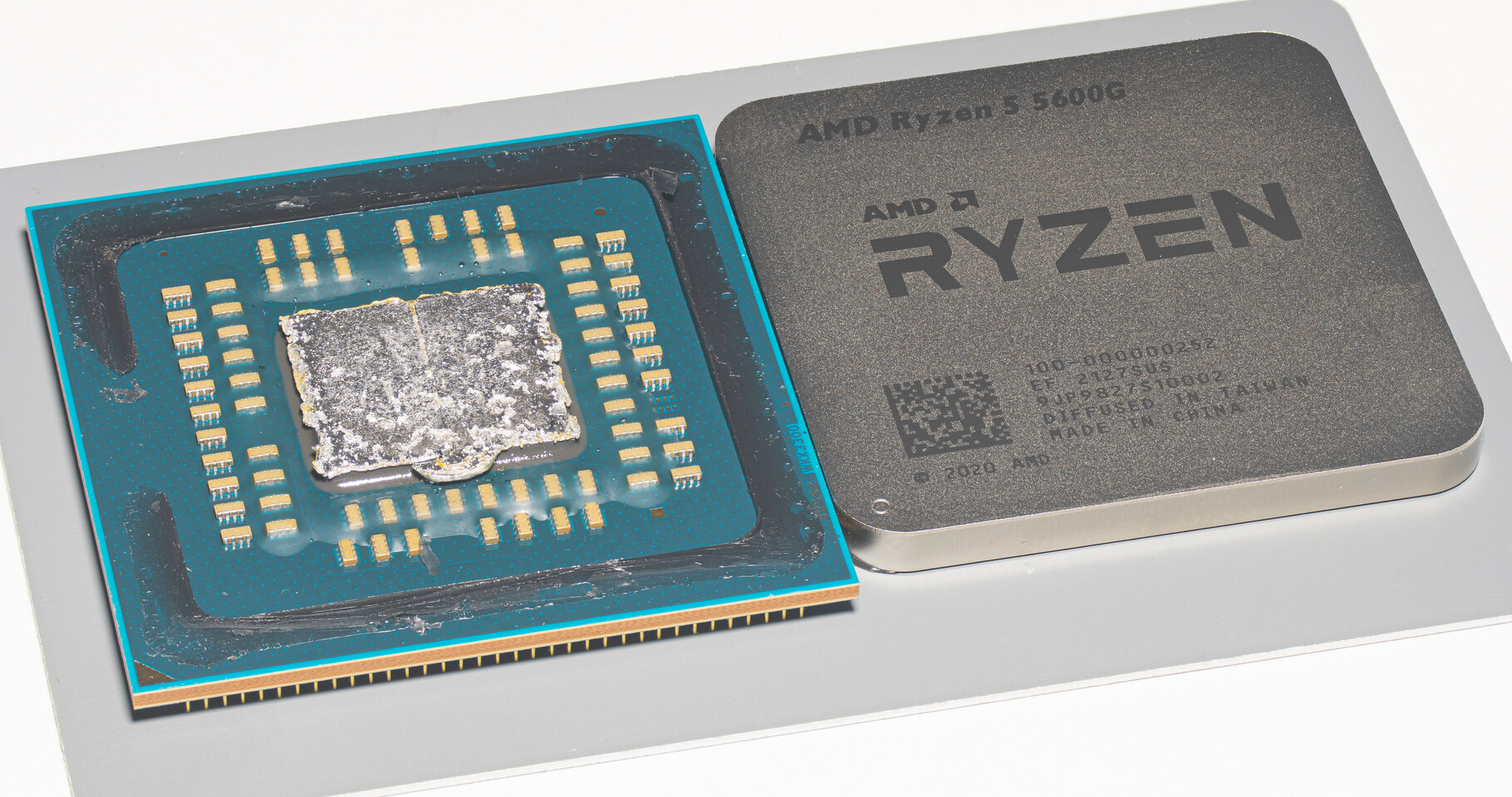
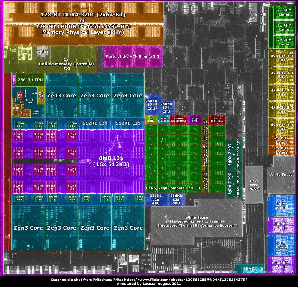
We have recently seen the first high-resolution die shots of AMD's Ryzen 5 5600G Cezanne APU thanks to the work of Fritzchens Fritz. The photos show the internal layout of the processor with its Zen 3 CPU, Vega GPU, and corresponding components. To get these shots, the chip had to be delidded by removing the IHS which has been made harder with the move to a soldered design. The Ryzen 5 5600G is a 6 core, 12 thread part with 7 Vega GPU cores which can all be seen in the annotated diagram of the die created by Locuza. The diagram also shows the suspected locations of various PCIe 3.0, and memory controllers along with cache placements for the CPU and GPU. The processor is manufactured on TSMC's 7 nm process and features a total of 10.7 Billion transistors packed into the 180 mm² die.


View at TechPowerUp Main Site
 
@Uskompuf I don't know who created that last die diagram, but that's for the 4650G/4750G. It literally says at the bottom of the image. The die shot itself, second last, is correct.

Interestingly enough, both the 5600G and 5700G I've gotten my hands on both have this weird square imprint in the middle of the heatspreader, demarcated by a thin line that basically forms a square over where the capacitor rows are. Not seen it on any other AM4 APU or CPU, doesn't seem to be residue either that can be wiped off. Seems like all the launch parts for Cezanne were made in the same week, 2127.

But yeah, nothing new. Good blob of paste in the middle like any other monolithic chip, and off to the races. So far the cores seem to run about the same temp as Renoir, are much more consistent core-to-core (unlike chiplet Zen 3 where I've seen upwards of 10C core deltas), and as always Vega 7/8 stays cool as ever even at 2300MHz+.

@R0H1T in case it wasn't obvious, they just delved further into one of the cores to show you its component parts..........not that it matters since it's the wrong APU.
 
It's clearly wrong, one half of the cores has unified L3 & the other doesn't! Also 3 cores, phenom X3 :slap: :laugh:
 
So it has 7 cores :wtf:
LvQhmWEzMHBgKVsp.jpg

No, that first core just has the individual components inside it labeled. Same with the first CU on the GPU and the first 4MB bank of L3 cache.

Look closely at the cores, cache, and CUs with detailed labeling, and you'll see that they all have identical layouts to the others.

Also @Uskompuf, the labeled image on the OP is of Renoir, not Cezanne.

Here's the labeled image for the Cezanne die.

AMD-Ryzen-5000G-Cezanne-Ryzen-4000G-Renoir-Die-Shot-Comparison-_3-1480x1430.jpg
 
Last edited:
Did they misused the 4750G die shot ?
The last one had 2 ccx
 
Here are the Cezanne and Renoir dies side-by-side for comparison.

AMD-Ryzen-5000G-Cezanne-Ryzen-4000G-Renoir-Die-Shot-Comparison-_3-1480x1430.jpg
LvQhmWEzMHBgKVsp.jpg


Note the identical GPU layout and the lack of a gap in the cores on Cezanne.

I also find the amount of unused space on Cezanne to be interesting. They needed a bigger die for the larger CPU component, but didn't have enough stuff to fill the extra space that it left them with.
 
Last edited:
in case it wasn't obvious, they just delved further into one of the cores to show you its component parts..........not that it matters since it's the wrong APU.
Yes just saw the updated labels for Cezanne, I forgot Renoir was the previous gen's codename.
 
Here are the Cezanne and Renoir dies side-by-side for comparison.

Note the identical GPU layout and the lack of a gap in the cores on Cezanne.

AIDA seems to think that the UMC is new. From the die shot the memory controllers look a little bit different.

5700g 48.0ns.png
4200 tightest timings.png


But aside from that, holy they weren't kidding when they said they just made a bunch of "optimizations". I was previously speculating that they literally drag-and-drop Zen 3 into Renoir, literally nothing changed on the GPU/IF side. Which is pretty much the experience so far, everything down to the CLDOs and VDDCR_GFX works the same way, only things different relate to the Zen 3 cores (Curve Optimizer). When not CPU-limited Vega 7 behaves the exact same.

And they added a iGPU Curve Optimizer as well, works basically the same way, but pretty much useless given the Vega core speeds that every 5600G/5700G seems to be able to hit manually.
 
Comparing these images has given me some interesting insight on CPU design.

Look at the unlabeled component below the GPU on Renoir; notice how the unused area on Cezanne has the same shape as it, and how that component is lower on that die? Also, note the gap underneath the PCIe lanes that doesn't exist on Renoir.

And as @tabascosauz pointed out, Cezanne does have a different IMC. The other support components look the same. They were just moved around to accommodate the larger CPU.
 
@Uskompuf I don't know who created that last die diagram, but that's for the 4650G/4750G. It literally says at the bottom of the image. The die shot itself, second last, is correct.

You are right the old one accidentally got put in during editing, the post has been updated.
 
AIDA seems to think that the UMC is new. From the die shot the memory controllers look a little bit different.

View attachment 212368 View attachment 212369

But aside from that, holy they weren't kidding when they said they just made a bunch of "optimizations". I was previously speculating that they literally drag-and-drop Zen 3 into Renoir, literally nothing changed on the GPU/IF side. Which is pretty much the experience so far, everything down to the CLDOs and VDDCR_GFX works the same way, only things different relate to the Zen 3 cores (Curve Optimizer). When not CPU-limited Vega 7 behaves the exact same.

And they added a iGPU Curve Optimizer as well, works basically the same way, but pretty much useless given the Vega core speeds that every 5600G/5700G seems to be able to hit manually.
Something has changed for sure as I can reach DDR4-5000/2500MHz 1:1 on 5700G and my last 4650G was hitting a wall at ~4600.
 

Attachments

  • 5k1.jpg
    5k1.jpg
    240.8 KB · Views: 228
The yields are not as high as tsmc advertised or is the sram taking most of the space
 
Something has changed for sure as I can reach DDR4-5000/2500MHz 1:1 on 5700G and my last 4650G was hitting a wall at ~4600.

The six-cores have never been on the same binning level as the 8-core, most 4650G were pretty meh on OC. My 5700G kinda scrapes by at 4400 with 2300MHz Vega 8, the 5600G refused to POST 2200Mhz on two different boards. I could kind of bench at 4400 with 2275MHz Vega 7 on the 4650G.

I'm assuming you're on a dGPU? @glnn_23 got up to about 4800 16-16-16, but I suppose B-die timings aren't helping us either. I wish I had a good kit of Rev.B on hand, but it would no longer be an apples-to-apples comparison as I sent the 5600G back.
From what I know, better Ryzen 4000 were limited to about ~4600 1:1. The same for 6 and 8 cores. 8 cores were going up better on the CPU cores but not really on the IMC. Or at least this is what I saw in my tests and around the web. My last 4650G was generally beating most 4750G. I was pushing 4650G up to DDR4-5400 CL18 stable with Micron IC 1:2 (can't find a screenshot now, only found older at 5300 CL18) and up to 5800 for quick benchmarks so IMC wasn't bad but at 1:1 it was 4533 max stable and 4600 for benchmarks.
How high it works highly depends on the motherboard. I had the best results on Strix B550I-Gaming. It was about 1-2 memory ratios better (depends on the memory kit) than CHVIII Impact or any other board that I tested.

The attached screenshot is on CHVIII Impact. It doesn't support IGP so I had to use a discrete one. So far I have had no time to check different IC so only Micron B in tests. I always had problems passing DDR4-4866 on a pretty good Samsung. Generally, for high clocks, APUs like Micron on ambient temps.
 
AIDA seems to think that the UMC is new. From the die shot the memory controllers look a little bit different.

But aside from that, holy they weren't kidding when they said they just made a bunch of "optimizations". I was previously speculating that they literally drag-and-drop Zen 3 into Renoir, literally nothing changed on the GPU/IF side. Which is pretty much the experience so far, everything down to the CLDOs and VDDCR_GFX works the same way, only things different relate to the Zen 3 cores (Curve Optimizer). When not CPU-limited Vega 7 behaves the exact same.

And they added a iGPU Curve Optimizer as well, works basically the same way, but pretty much useless given the Vega core speeds that every 5600G/5700G seems to be able to hit manually.

You should test with locked cpu freqs. The mem speed and mem latency tests are very single cpu bound.
 
Ugh, the ratio of CPU to GPU cores in these products still offends me.

1628856067679.png


They could chop off two CPU cores and 1/4 the L3 cache to give that space to probably another 12 Vega CUs.

6C/12T with Vega20 would be a far better product than 8C/12T with cripplingly-slow graphics. Here's a quick-n-dirty 6C/12T Vega20 mockup just shuffling a few blocks around with minimal overlap:

1628856527180.png
 
Last edited:
No, that first core just has the individual components inside it labeled. Same with the first CU on the GPU and the first 4MB bank of L3 cache.

Look closely at the cores, cache, and CUs with detailed labeling, and you'll see that they all have identical layouts to the others.

Also @Uskompuf, the labeled image on the OP is of Renoir, not Cezanne.

Here's the labeled image for the Cezanne die.

AMD-Ryzen-5000G-Cezanne-Ryzen-4000G-Renoir-Die-Shot-Comparison-_3-1480x1430.jpg

So this pic has no vega cores disabled, but two Zen 3 cores disabled then?

Otherwise this is an 8c16t or am I on drugs
 
Ugh, the ratio of CPU to GPU cores in these products still offends me.

View attachment 212389

They could chop off two CPU cores and 1/4 the L3 cache to give that space to probably another 12 Vega CUs.

6C/12T with Vega20 would be a far better product than 8C/12T with cripplingly-slow graphics. Here's a quick-n-dirty 6C/12T Vega20 mockup just shuffling a few blocks around with minimal overlap:

View attachment 212390
Spot on, but I think thermals are the issue. It would be easy to dump 120W out with double the GPU, and then there is also the memory bandwidth issue.
 
Nah, that doesn't really work with DDR4 memory bandwidth, the GPU cores would just be memory starved at that point.
 
So this pic has no vega cores disabled, but two Zen 3 cores disabled then?

Otherwise this is an 8c16t or am I on drugs


Yeah, I wasn't aware that AMD had enough demand to justify a 6-core native part? Only Intel has pulled that in the past (Coffee Lake)
 
I'm thinking LSD, or you're more of an instant pot guy?

Still counting 8 cores though and not 6.

Also an 8th vega in there, btw
 
Nah, that doesn't really work with DDR4 memory bandwidth, the GPU cores would just be memory starved at that point.
Plenty of proof showing that more CUs would give more performance. Sure, DDR4 bandwidth sucks, but the limitation of current IGPs is still the lack of CUs. Additionally, we're now at the point where AMD's APUs support 3600MHz+ RAM speeds, and 1st-gen Zen APUs were struggling to get beyond 2666MHz until several AGESA revisions later. There's 35% more bandwidth to feed 35% more CUs right there from IMC and DDR4 speeds alone!
Spot on, but I think thermals are the issue. It would be easy to dump 120W out with double the GPU, and then there is also the memory bandwidth issue.
Mobile parts with Vega8 at 15W (actually more like 30W under boost loads) - so Vega20 doesn't have to be a 120W part. Restrict the IGP to 50W and you could still probably get 2GHz out of that integrated GPU.

Hell I don't know, even Vega12 would be an improvement, we just don't get enough GPU power in these things and the only reason people are buying them instead of the regular Zen3 chips is because they want the GPU included.
 
Back
Top