• Welcome to TechPowerUp Forums, Guest! Please check out our forum guidelines for info related to our community.

TSMC 3 nm To Enter Volume Production in 2022

btarunr

Editor & Senior Moderator
Staff member
Joined
Oct 9, 2007
Messages
47,886 (7.38/day)
Location
Dublin, Ireland
System Name RBMK-1000
Processor AMD Ryzen 7 5700G
Motherboard Gigabyte B550 AORUS Elite V2
Cooling DeepCool Gammax L240 V2
Memory 2x 16GB DDR4-3200
Video Card(s) Galax RTX 4070 Ti EX
Storage Samsung 990 1TB
Display(s) BenQ 1440p 60 Hz 27-inch
Case Corsair Carbide 100R
Audio Device(s) ASUS SupremeFX S1220A
Power Supply Cooler Master MWE Gold 650W
Mouse ASUS ROG Strix Impact
Keyboard Gamdias Hermes E2
Software Windows 11 Pro
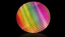
TSMC will commercialize its N3 (3 nm) EUV silicon fabrication node in 2022, with volume production set to commence in the second half of the year. The company is looking to maximize capacity on its current N5 (5 nm) node, which already serves major customers such as Apple. AMD is expected to utilize N5 allocation going into 2022 as its next-generation "Zen 4" processors are expected to leverage the node to drive up CPU core counts and caches. The company is also utilizing N6 (6 nm) for its CDNA2 compute accelerator logic dies. N5 could also power mobile application processors from several manufacturers.


View at TechPowerUp Main Site
 
Now, if only the supply would keep up... Otherwise, yay tech progress go!
 
I didn't think 3nm was physically possible?
 
Now, if only the supply would keep up... Otherwise, yay tech progress go!
These are only going to Apple, maybe Intel ~ if they pay for it. There's also rumors that Apple will switch to ARM for its servers so expect the leading edge to be even more scarce in the future!
 
Here we go....people being confused by the single nano-meter number again... :kookoo:
 
20nm, 25nm, 30nm or larger!
Not sure I'd go that far but it has indeed become a meaningless number race.
 
I didn't think 3nm was physically possible?
An old man comes to a doctor and says:
-My neighbor is 85, but he says he's having sex 3 times a day. I am 84 and can't even once a quarter.
-Nah, says the doctor, you can also say you are having sex 3 times a day just as well as he does.
 
Who for, Apple? AMD will be lucky to get any of that.
 
Again, blatant marketing lies from TSMC.
Here is the best explanation so far:

Samsung’s 10nm and 7nm nodes were both on par with TSMC’s, at least in terms of transistor density, packing 0.52 and 0.95 million transistors per square mm. Meanwhile, Intel’s 10nm node was denser than both, with a density of 1.06 million per square mm. Starting with the 5nm node, Samsung’s nodes have fallen behind. The Korean foundry’s 5nm node has a transistor density of 1.27 million (per mm2), compared to 1.73 million on TSMC’s 5nm and 1.8 million on Intel’s 7nm.

The deltas become even wider with the 3nm node, with Samsung expected to offer a density of just 1.7 million, compared to 2.9 million on TSMC’s 3nm (despite not using GAA), and 3 million on Intel’s 3nm.
 
Again, blatant marketing lies from TSMC.
Here is the best explanation so far:
The density is actually 100 times as much. Look at the graph, which is properly annotated ("Unit : 100million/square mm").

Still, at 100 MTr/mm², an average transistor measures around 100 nm x 100 nm, so the finest structures, and spacing between them, are probably 15-20 nm wide.

To TSMC's credit, they prefer to talk about node names, like N3 and N4, and avoid mentioning nanometers. Likewise for Samsung (7LPP and such) and lately Intel.
 
Go TSMC, bring it :)
 
Again, blatant marketing lies from TSMC.
Here is the best explanation so far:
You forgetting the most blatant lie spread by the Intel's marketing team and fans. On paper and test chip density vs real chip density. Intel may have higher on paper density, but on real chip Intel is sometimes behind the GlobalFoundaries older node. GloFlo's 28nm SPH has higher density then Intel's 22nm 2nd gen. [AMD Kaveri, 28nm SHP, 2.41B, 245mm2, 9.83 M/mm2][Intel Haswell-S/GT2, 22nm FinFET, 1.4B, 177mm2, 7.9M/mm2]
 
A lot of folks are misusing process information to make various vendors appear to be ahead/behind.

Calling 10nm, 7nm this-or-that, or visa versa makes us all look basic af. Processor gate production, today, is at the nanometer measurement scale.

The switch from one type of production process to the next (FinFET to gate-all-around) has overlap. Moore's Law isn't dead..yet.

Great current-state writeup here if you're actually into facts:

https://semiengineering.com/new-transistor-structures-at-3nm-2nm/
 
Transistor speed and power consumption are more important than density

You forgetting the most blatant lie spread by the Intel's marketing team and fans. On paper and test chip density vs real chip density. Intel may have higher on paper density, but on real chip Intel is sometimes behind the GlobalFoundaries older node. GloFlo's 28nm SPH has higher density then Intel's 22nm 2nd gen. [AMD Kaveri, 28nm SHP, 2.41B, 245mm2, 9.83 M/mm2][Intel Haswell-S/GT2, 22nm FinFET, 1.4B, 177mm2, 7.9M/mm2]
Plus intel hides transistor count from the public... it's like they hiding something from people
 
Good write up. Thanks for sharing it.

Reading it made me come to conclusion that I shouldn't expect TSMC/Samsung 5 nm GPUs anytime in the near future. Those bleeding edge nodes will be preferred for CPU chiplets and Smartphone SoCs. GPUs are simply way too big. The 2 smallest chips from Nvidia and AMD right now - GA107 and Navi 23 - are big boys at ~190 mm² and ~240 mm² respectively.

To put things in perspective, Cezanne - AMD's SoC with Eight Zen 3 cores and a iGPU - is only 180 mm². Apple's A13 is around 100 mm².
 
Last edited:
They are behind schedule I think? 2nd half of the year means they will miss the Apple iPhone 14 window. Maybe we will have iPhone 13S instead.

Also, between now and 2H2022, Zen 3 will need top drop prices to stay competitive with Intel's aggressive prices, instead of rushing to Zen 4: is this a win in disguise?
 
Back
Top