TheLostSwede
News Editor
- Joined
- Nov 11, 2004
- Messages
- 18,835 (2.50/day)
- Location
- Sweden
| System Name | Overlord Mk MLI |
|---|---|
| Processor | AMD Ryzen 7 7800X3D |
| Motherboard | Gigabyte X670E Aorus Master |
| Cooling | Noctua NH-D15 SE with offsets |
| Memory | 32GB Team T-Create Expert DDR5 6000 MHz @ CL30-34-34-68 |
| Video Card(s) | Gainward GeForce RTX 4080 Phantom GS |
| Storage | 1TB Solidigm P44 Pro, 2 TB Corsair MP600 Pro, 2TB Kingston KC3000 |
| Display(s) | Acer XV272K LVbmiipruzx 4K@160Hz |
| Case | Fractal Design Torrent Compact |
| Audio Device(s) | Corsair Virtuoso SE |
| Power Supply | be quiet! Pure Power 12 M 850 W |
| Mouse | Logitech G502 Lightspeed |
| Keyboard | Corsair K70 Max |
| Software | Windows 10 Pro |
| Benchmark Scores | https://valid.x86.fr/yfsd9w |
According to an article by DigiTimes, which kind of states the obvious, the foundry industry isn't likely to change much over the next few years, as the cost of building a cutting edge foundry keeps increasing, which means the competition isn't likely to catch up with the market leaders. The costs mentioned are estimates, but seem quite likely and explains why there's so little competition in the foundry business.
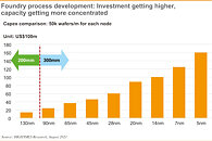
It's unclear if the costs have been inflation adjusted or not, but a 90 nm 12-inch fab that could output 50,000 wafers a month, is said to have cost US$2.4 billion to build when it was the cutting edge node. Once things moved on to 28 nm, the equivalent fab would've cost US$6 billion, whereas a cutting edge 5 nm fab today, comes in at as much as US$16 billion. These are obviously long term investments, as even today, 90 nm nodes are used for plenty of chips, but most of the nodes above 28 nm are today used for specialty products rather than commonly used ICs, unless we're talking about 8-bit microcontrollers or some simpler components which companies such as TSMC and Samsung wouldn't even bother making.
The article continues to mention that TSMC is set to re-invest around 54 percent of its revenue from this year into building new fabs and nodes. It should also be noted that TSMC is making some 52 percent of its revenue from its most advanced nodes, with 5 nm being around 18 percent and 7 nm 34 percent, according to Bloomberg. The last quarter of 2021, TSMC is expected to pull in a revenue of US$15.7 billion, which should be compared to Samsung's foundry business that isn't expected to break the US$15 billion mark this year.
DigiTimes seem to think that TSMC has an advantage over Samsung due to TSMC's much greater revenue, but seems to have forgotten that the Samsung foundry business has the rest of Samsung behind it as well and the company as a whole pulled in some US$63 billions in revenue in the third quarter of this year. Samsung might be willing to invest a fair chunk of that change into its foundry business to stay competitive, least not because Samsung is relying heavily on its own foundry business, not only for mobile SoCs, but also for its storage products. As to how much profit Samsung is earning on its third party foundry business at this point is unclear, but it seems to become increasingly important as Samsung moves to smaller and smaller nodes.
As to where things will end up, is anyone's guess at this point, but with these kinds of investments required for every cutting edge foundry, it's no wonder that these companies are looking for every bit of extra financial support that they can get when they're looking at where to build their next foundry. We're unlikely to see a move away from semiconductors any time soon and node shrinks are proving just as important as everything else that goes into making advanced chips, so as long as someone is willing to invest, we're going to continue to see regular node shrinks, although it's likely that the cost of new fabs are going to be the cause for a slowdown before we got to the point where the various technologies used to make chips are becoming the limiting factor.
View at TechPowerUp Main Site
It's unclear if the costs have been inflation adjusted or not, but a 90 nm 12-inch fab that could output 50,000 wafers a month, is said to have cost US$2.4 billion to build when it was the cutting edge node. Once things moved on to 28 nm, the equivalent fab would've cost US$6 billion, whereas a cutting edge 5 nm fab today, comes in at as much as US$16 billion. These are obviously long term investments, as even today, 90 nm nodes are used for plenty of chips, but most of the nodes above 28 nm are today used for specialty products rather than commonly used ICs, unless we're talking about 8-bit microcontrollers or some simpler components which companies such as TSMC and Samsung wouldn't even bother making.

The article continues to mention that TSMC is set to re-invest around 54 percent of its revenue from this year into building new fabs and nodes. It should also be noted that TSMC is making some 52 percent of its revenue from its most advanced nodes, with 5 nm being around 18 percent and 7 nm 34 percent, according to Bloomberg. The last quarter of 2021, TSMC is expected to pull in a revenue of US$15.7 billion, which should be compared to Samsung's foundry business that isn't expected to break the US$15 billion mark this year.
DigiTimes seem to think that TSMC has an advantage over Samsung due to TSMC's much greater revenue, but seems to have forgotten that the Samsung foundry business has the rest of Samsung behind it as well and the company as a whole pulled in some US$63 billions in revenue in the third quarter of this year. Samsung might be willing to invest a fair chunk of that change into its foundry business to stay competitive, least not because Samsung is relying heavily on its own foundry business, not only for mobile SoCs, but also for its storage products. As to how much profit Samsung is earning on its third party foundry business at this point is unclear, but it seems to become increasingly important as Samsung moves to smaller and smaller nodes.
As to where things will end up, is anyone's guess at this point, but with these kinds of investments required for every cutting edge foundry, it's no wonder that these companies are looking for every bit of extra financial support that they can get when they're looking at where to build their next foundry. We're unlikely to see a move away from semiconductors any time soon and node shrinks are proving just as important as everything else that goes into making advanced chips, so as long as someone is willing to invest, we're going to continue to see regular node shrinks, although it's likely that the cost of new fabs are going to be the cause for a slowdown before we got to the point where the various technologies used to make chips are becoming the limiting factor.
View at TechPowerUp Main Site


")