• Welcome to TechPowerUp Forums, Guest! Please check out our forum guidelines for info related to our community.
  • The forums have been upgraded with support for dark mode. By default it will follow the setting on your system/browser. You may override it by scrolling to the end of the page and clicking the gears icon.

Intel "Meteor Lake" and "Arrow Lake" Use GPU Chiplets

btarunr

Editor & Senior Moderator
Staff member
Joined
Oct 9, 2007
Messages
47,804 (7.40/day)
Location
Dublin, Ireland
System Name RBMK-1000
Processor AMD Ryzen 7 5700G
Motherboard Gigabyte B550 AORUS Elite V2
Cooling DeepCool Gammax L240 V2
Memory 2x 16GB DDR4-3200
Video Card(s) Galax RTX 4070 Ti EX
Storage Samsung 990 1TB
Display(s) BenQ 1440p 60 Hz 27-inch
Case Corsair Carbide 100R
Audio Device(s) ASUS SupremeFX S1220A
Power Supply Cooler Master MWE Gold 650W
Mouse ASUS ROG Strix Impact
Keyboard Gamdias Hermes E2
Software Windows 11 Pro
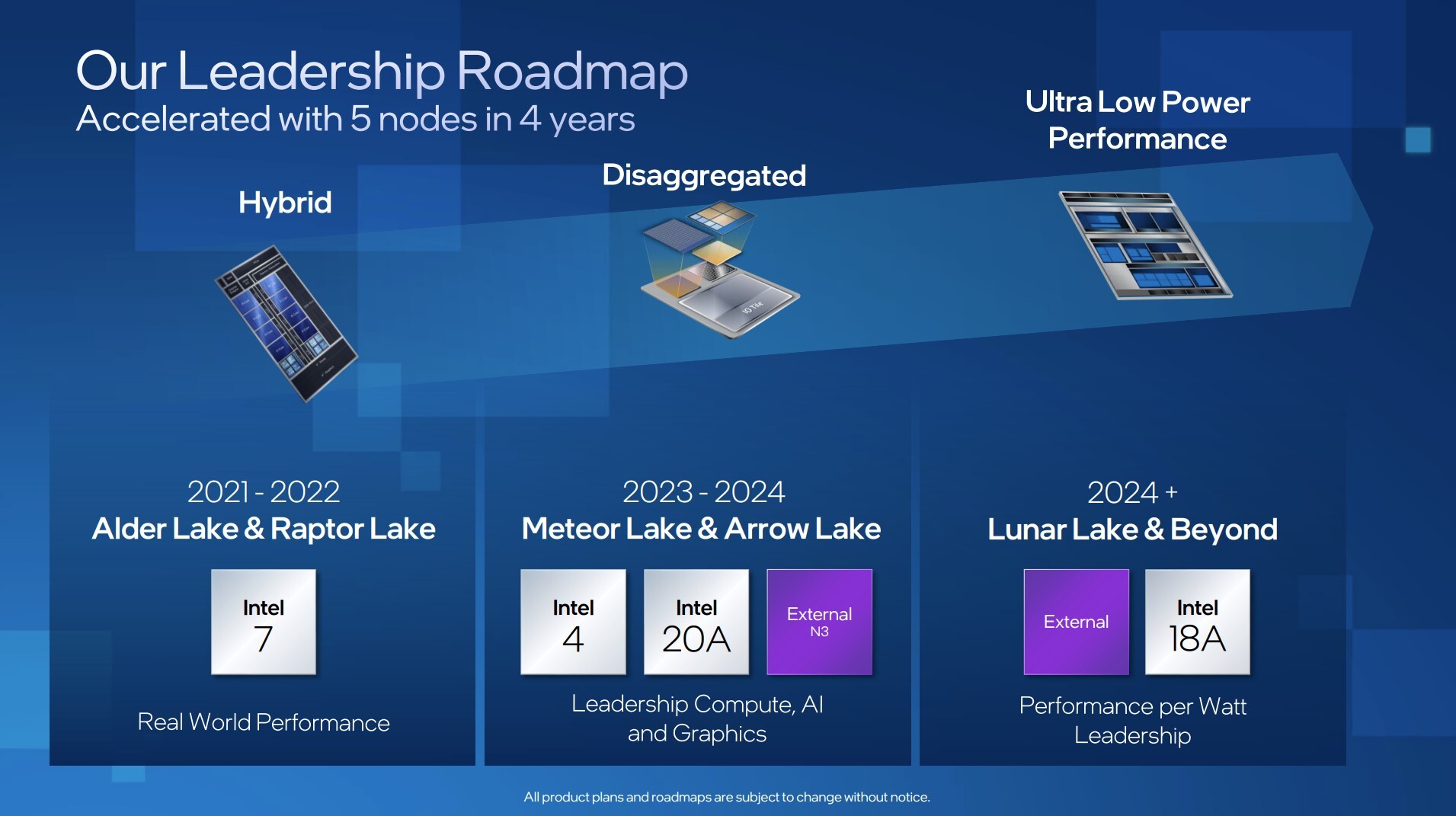
Intel's upcoming "Meteor Lake" and "Arrow Lake" client mobile processors introduce an interesting twist to the chiplet concept. Earlier represented in vague-looking IP blocks, new artistic impressions of the chip put out by Intel shed light on a 3-die approach not unlike the Ryzen "Vermeer" MCM that has up to two CPU core dies (CCDs) talking to a cIOD (client IO die), which handles all the SoC connectivity; Intel's design has one major difference, and that's integrated graphics. Apparently, Intel's MCM uses a GPU die sitting next to the CPU core die, and the I/O (SoC) die. Intel likes to call its chiplets "tiles," and so we'll go with that.

The Graphics tile, CPU tile, and the SoC or I/O tile, are built on three different silicon fabrication process nodes based on the degree of need for the newer process node. The nodes used are Intel 4 (optically 7 nm EUV, but with characteristics of a 5 nm-class node); Intel 20A (characteristics of 2 nm), and external TSMC N3 (3 nm) node. At this point we don't know which tile gets what. From the looks of it, the CPU tile has a hybrid CPU core architecture made up of "Redwood Cove" P-cores, and "Crestmont" E-core clusters.


The Graphics tile packs an iGPU based on the Xe LP graphics architecture, but leverages an advanced node to significantly increase the execution unit (EU) count to 352, and possible increase graphics clocks. The SoC and I/O tile packs the platform security processor, integrated northbridge, memory controllers, PCI-Express root-complex, and the various platform I/O.

Intel is preparing "Meteor Lake" for a 2023 launch, with development completing within 2022, although mass-production might still commence next year.

View at TechPowerUp Main Site
 
I can't believe they're spinning this as new , I mean a reasonably useful GPU in an Intel CPU would be new, but Intel doing an McM with a CPU and GPU is so last decade.

And a few weeks ago they were buying their competitors GPU to place on their McM.(sarcasm :p)

In fact the only new bit is Intel has decided to nick AMD'S McM IO die concept, no?!.
 
Gets me excited for my next upgrade, which will definitely be Nova Lake or later. Zero reason to ditch my 5900X before that major change.
 
Intel must have sniffed the glue from when AMD started with CCDs.
 
My 90nm identifies as 1nm and failure to respect that is hate crime.
 
In fact the only new bit is Intel has decided to nick AMD'S McM IO die concept, no?!.

Clarkdale had a separate die that had the iGPU and IMC back in 2010.

The CPU die was based on a 32nm process while the iGPU die was 45nm.


L_00013090.jpg
 
So Intel had the great idea of chiplets/tiles as early as clarkdale in 2010, did they go back to a single die after this? If so I wonder why. As long as the interconnect between them is fast enough it's a great setup as seen by Ryzen.

What is the interface between the tiles on these?
 
Clarkdale had a separate die that had the iGPU and IMC back in 2010.

The CPU die was based on a 32nm process while the iGPU die was 45nm.


L_00013090.jpg
I was about to say the same thing: the Kaby Lake Xeon E3 1535M v6 in my HP zbook 17 G4 has the same config (CPU die + GPU die). So nothing new, except Intel becomes more friendly with glue. Competition is always good.
 
Kaby Lake with Radeon is the closest to what these are, but unlike those this should be all part of the same package rather than being multiple chips on the same PCB. This should be similar to the SPR tiles, but in this case the CPU/IO/GPU may very well be on three different process nodes (assuming GPU will be TSMC). Packaging is rapidly looking like it is going to be as important as the process nodes themselves.
 
Intel's got an R&D budget 650% larger than AMD's and look who's engineering they're copying
 
I like how easily the highly educated mob of TPU thinks on-die chiplets and on-substrate chiplets are the same thing.

Stay classy, armchair TPU engineers.
Can you explain what you mean by on-die chiplets?
 
I like how easily the highly educated mob of TPU thinks on-die chiplets and on-substrate chiplets are the same thing.

Stay classy, armchair TPU engineers.
So snarky, i like it.
Can you explain what you mean by on-die chiplets?
What, haven't you heard about Intel's superior EMIB glue? It works great, especially on PPT slides.
 
Last edited:
Can you explain what you mean by on-die chiplets?
It means different IPs connect to each-other with a much faster, much lower latency compared to substrate solutions that existed so far for chiplet to chiplet interconnect.
Combining different IPs from different nodes together to work as if it was a monolithic design has the bandwidth advantage to it. That means more data per per given time frame.
 
So the work AMD put into silicon interconnects gets reused by Intel?
 
So the work AMD put into silicon interconnects gets reused by Intel?
It's fair to say everyone was/is working on that already.
And Intel's way of doing Emib certainly differs from anyone else's.
 
It means different IPs connect to each-other with a much faster, much lower latency compared to substrate solutions that existed so far for chiplet to chiplet interconnect.
Combining different IPs from different nodes together to work as if it was a monolithic design has the bandwidth advantage to it. That means more data per per given time frame.
I just never thought of EMIB as "die" but a small buried silicon interposer. But Intel says it is a "very small bridge die", so it is a die. (The description is hard to follow because Intel thinks the plural of die is die.)

I too think that it's going to be very good but let's wait and see how it performs in Sapphire Rapids. It's supposed to integrate the four chips so tightly as to make any interface logic unnecessary. It would result in lower latency but lower power consumption is equally important.
 
So Intel had the great idea of chiplets/tiles as early as clarkdale in 2010, did they go back to a single die after this? If so I wonder why. As long as the interconnect between them is fast enough it's a great setup as seen by Ryzen.
Intel did go back to a monolithic die after Clarkdale with Westmere and Sandy Bridge.

img_0135-jpg.743369


Here's a delidded Westmere CPU, an X5690, from early 2011.

I think Clarkdale did have issues with latency.

Didn't Zen 2 also have issues with latency between the different core clusters?

EDIT: Apparently the old Core 2 Quads had multiple dies.

58710.jpg


Picture from @Ruslan

I knew that the older Pentium D chips also had multiple dies.

Both dies were processor dies. This was back in the days of having the northbridge on the motherboard.
 
Last edited:
I just never thought of EMIB as "die" but a small buried silicon interposer. But Intel says it is a "very small bridge die", so it is a die. (The description is hard to follow because Intel thinks the plural of die is die.)

I too think that it's going to be very good but let's wait and see how it performs in Sapphire Rapids. It's supposed to integrate the four chips so tightly as to make any interface logic unnecessary. It would result in lower latency but lower power consumption is equally important.
From my understanding, its not exactly the "same EMIB". There's gonna be some kooky new tweak to the interposer that's going to be used in those multi-IP franken-dies.
No concrete info on how exactly this technology is going to work.
 
That emib is very clever. Is that how AMD do it?
No there's use Tsmc through hole vias.
And then recently die on die Stiction pads.
 
With the multi-node die they're probably going to be leveraging Foveros if for no other reason than to make sure everything is level though there may be cache stacking as well to keep the compute tile size down. The interconnects themselves should be all EMIB similar to SPR.
 
Back
Top