• Welcome to TechPowerUp Forums, Guest! Please check out our forum guidelines for info related to our community.

Apple Mac Studio Taken Apart, Reveals Giant M1 Ultra SoC

btarunr

Editor & Senior Moderator
Staff member
Joined
Oct 9, 2007
Messages
47,680 (7.43/day)
Location
Dublin, Ireland
System Name RBMK-1000
Processor AMD Ryzen 7 5700G
Motherboard Gigabyte B550 AORUS Elite V2
Cooling DeepCool Gammax L240 V2
Memory 2x 16GB DDR4-3200
Video Card(s) Galax RTX 4070 Ti EX
Storage Samsung 990 1TB
Display(s) BenQ 1440p 60 Hz 27-inch
Case Corsair Carbide 100R
Audio Device(s) ASUS SupremeFX S1220A
Power Supply Cooler Master MWE Gold 650W
Mouse ASUS ROG Strix Impact
Keyboard Gamdias Hermes E2
Software Windows 11 Pro
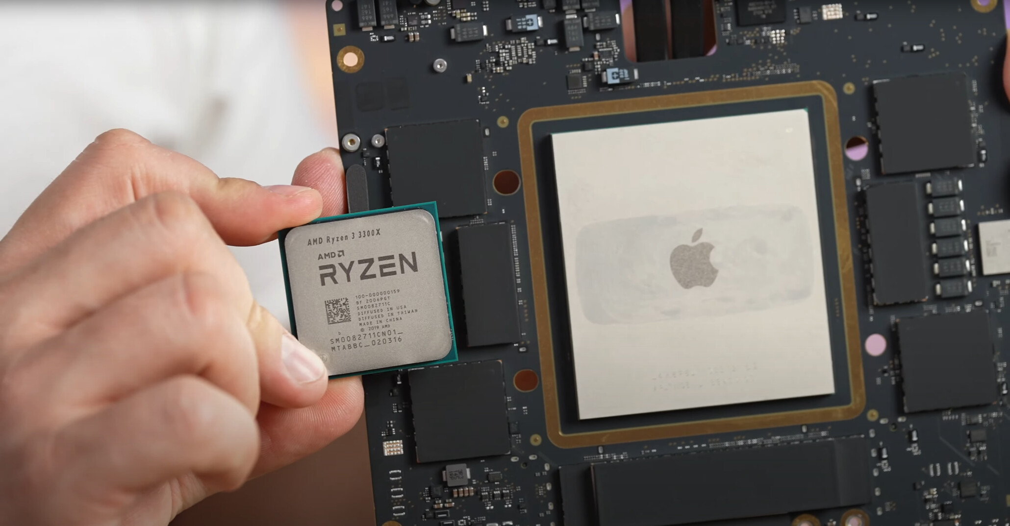
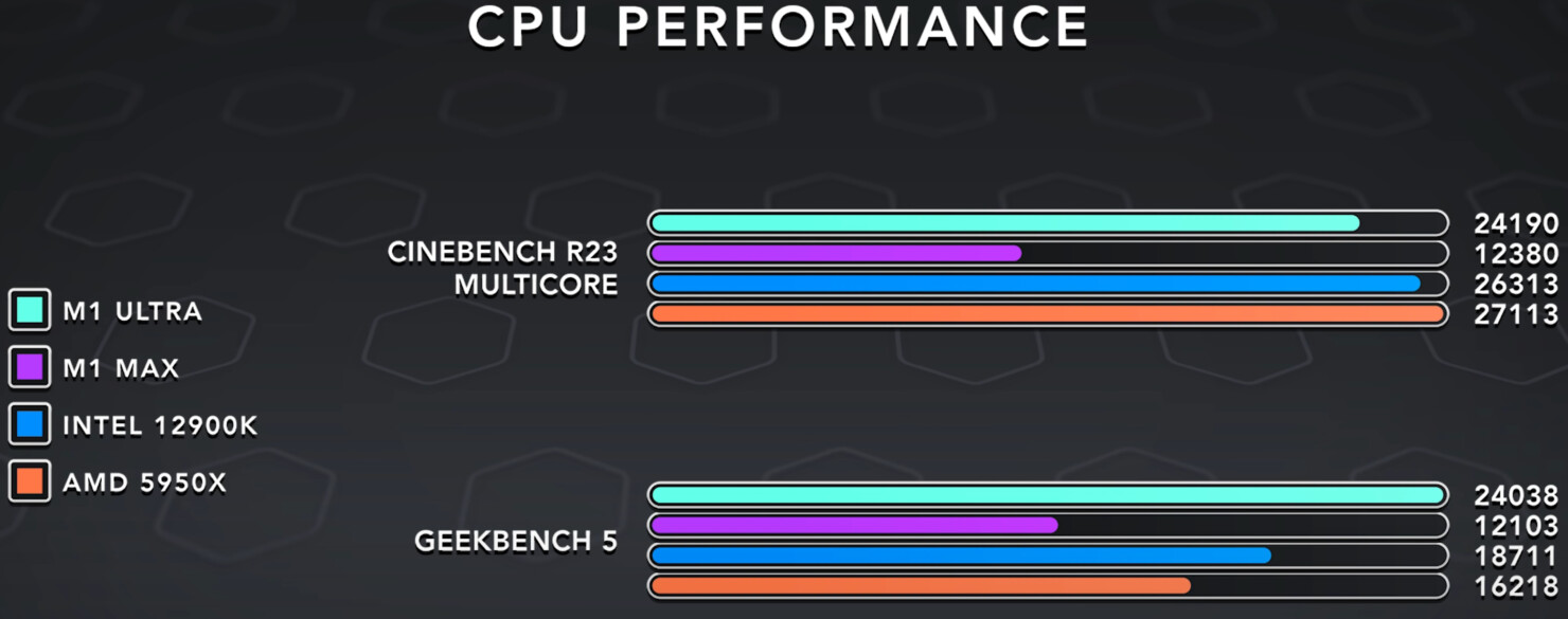
Max Tech performed the first detailed teardown of the Apple Mac Studio, the most powerful Mac since Apple dumped Intel for processors in favor of its own silicon based around high-performance Arm chips built from the ground-up for its own software ecosystem. The M1 Ultra SoC powering the Mac Studio is its most striking piece of technology, with Apple attaching some very tall performance claims not just for its CPU compute performance, but also graphics rendering performance.

The M1 Ultra SoC is physically huge, with roughly similar package size to an AMD EPYC processor in the SP3 package. An integrated heatspreader (IHS) covers almost the entire topside of the package. Things get interesting under the hood. The M1 Ultra is a multi-chip module of two M1 Max dies connected on package using Apple UltraFusion, a coherent fabric interconnect that allows the various components of the two M1 Max dies to access memory controlled by the other die. Speaking of memory, The M1 Ultra features up to 128 GB of LPDDR5 memory that's on-package, This memory is used for the CPU, GPU, as well as the neural processor, and has a combined memory bandwidth of 800 GB/s. The M1 Ultra features up to 20 CPU cores, up to 32 Neural cores, and up to 64 GPU cores (8,192 programmable shaders).


View at TechPowerUp Main Site | Source
 
Isn't Apple using TSMC N5 for this? That's even more so a honking big chunk of monolithic silicon. Even if the DRAM is included. Speculation said M1 was 120mm^2 ish, and M1 ultra is what, 8 times that?

AMD: moar cache
Intel: moar cores
Apple: moar die size

What a monster, huh. A Geekbench monster and not much else, that is :D
 
Last edited:
Guessing the larger die area indirectly grants increased energy efficiency.
 
Guessing the larger die area indirectly grants increased energy efficiency.
Say what?

Isn't Apple using TSMC N5 for this? That's even more so a honking big chunk of monolithic silicon. Even if the DRAM is included. Speculation said M1 was 120mm^2 ish, and M1 ultra is what, 8 times that?

AMD: moar cache
Intel: moar cores
Apple: moar die size

What a monster, huh. A Geekbench monster and not much else, that is :D
Not even HBM2... M-e-e-e-h!
 
What I want to see with TSV is like a 4 sided TSV connected cube of PCB's and then a another 4 inside in a cross shape design. Basically 8 PCB's that could contain circuitry that could be interconnected via TSV. I'd keep two edge ends open to allow for a push/pull blower configuration thru them though. I think eventually we could see something akin to these memory heatsink on each side of the PCB's connected via TSV wit chips on each side for the inner 4 cross shape in design mentioned with just enough excess area around them for TSV connections between them to others like them. Basically enough for a CPU chip die and memory on opposite side with heatsinks for both that can then be TSV interconnected to adjacent ones and cooled in a sort of blower chamber cube. The whole thing could pretty much be a modular TSV connection of PCB's with chips on each side sandwiched with heatsinks attached to them.

1647812211144.png

Isn't Apple using TSMC N5 for this? That's even more so a honking big chunk of monolithic silicon. Even if the DRAM is included. Speculation said M1 was 120mm^2 ish, and M1 ultra is what, 8 times that?

AMD: moar cache
Intel: moar cores
Apple: moar die size

What a monster, huh. A Geekbench monster and not much else, that is :D
It's closer to more heatspreader area than die size since it's several dies closely connected via TSV. I don't have a problem with that approach it's the right thing do for the time being if anything to keep yields manageable. I think really until we've gotten to a point where it's no longer practical and feasible to enlarge the socket size dimensions on a MB it still make the most sense since 3D stacking becomes a more tricky en-devour once you increase heat into the equation more readily eventually more of that concern can certain decrease at smaller nodes though. You can really randomize those three names with that moar x satire all three are pushing for more everything. It's funny how it started as just a poking fun satire of AMD's bulldozer missteps really and has just transformed over the years into a byproduct of the complications of chip making and perpectuation of our desire for them to do more of everything despite 640KB being all you need.
 
Last edited:
Isn't Apple using TSMC N5 for this? That's even more so a honking big chunk of monolithic silicon. Even if the DRAM is included. Speculation said M1 was 120mm^2 ish, and M1 ultra is what, 8 times that?

AMD: moar cache
Intel: moar cores
Apple: moar die size

What a monster, huh. A Geekbench monster and not much else, that is :D

It's faster than my 12700k, and faster than my RTX 3070. It's not bad. It's an expensive luxury product, but it isn't bad.

It can run Baldur's Gate 3 at 4k/60fps for example.

Also you are just looking at the integrated heat spreader. All the ram is under there. The actual chip is a lot smaller. And even then the SOC can't be compared against a plain CPU or GPU, there's a lot of cache and other things that take space. 16GB DDR5 has more transistors than the M1 Ultra, and more than any CPU, for example. Ever added up the area of all the ICs you can see on a plain ram stick?
 
Intel, AMD, Qualcomm have created an interconnect alliance, probably because they're scared that the rich boy is just throwing money at the problem. That package size is ridiculous, likely matched only by how ridiculous Apple's profit margins are.
 
Intel, AMD, Qualcomm have created an interconnect alliance, probably because they're scared that the rich boy is just throwing money at the problem. That package size is ridiculous, likely matched only by how ridiculous Apple's profit margins are.

The "CPU package" not including the memory is 1/3 the size of the IHS. It isn't that big. You can tell by the thermal paste only covering a third of it.
 
It's faster than my 12700k, and faster than my RTX 3070. It's not bad. It's an expensive luxury product, but it isn't bad.

It can run Baldur's Gate 3 at 4k/60fps for example.

Also you are just looking at the integrated heat spreader. All the ram is under there. The actual chip is a lot smaller. And even then the SOC can't be compared against a plain CPU or GPU, there's a lot of cache and other things that take space. 16GB DDR5 has more transistors than the M1 Ultra, and more than any CPU, for example. Ever added up the area of all the ICs you can see on a plain ram stick?

A12700k is 22k stock MC on R23 so not that much faster.
 
I would bet money the M1 is nothing more but an AMD cpu with the name scratched off and the Apple logo printed on it. Apple has done that in the past.
 
A12700k is 22k stock MC on R23 so not that much faster.

That's the problem right? Modified phone processor catching up to a desktop-first chip, backed by the biggest mountain of cash in the corporate world. Intel is the underdog here, their market cap is 1/10th the size of Apple's.
 
Apple will always say it's faster than anything on the market but never tells you in what it is faster at. All the media its faster than this faster then that but in what it never tells you.
 
48Mb of L2 cache is a lot of cache for 20
cores, maybe we have reached the pleateau of custom silicon and need to start integrating more cache for more performance. I’m curious about the latency, maybe we will see numbers.

All current general purpose tests show it’s slower overall than 1 or 2 generation old hardware X86-64, but for specific tests it’s still equal to current iteration hardware, 3D stack from AMD may be faster
 
wondering if hbm3 will make its way to M2.
 
Apple needs some Trojan Magnum's, damn.
 
A12700k is 22k stock MC on R23 so not that much faster.
Not sure I understand your comment. I said it is faster. You agree. But it isn't that much faster. Ok. It is 15 percent faster. ;)
 
Apple will always say it's faster than anything on the market but never tells you in what it is faster at. All the media its faster than this faster then that but in what it never tells you.
That's not true at all. All you have to do is scroll down to the bottom of the page and read the details they have provided for you to read.
 
Last edited:
What I want to see with TSV is like a 4 sided TSV connected cube of PCB's and then a another 4 inside in a cross shape design. Basically 8 PCB's that could contain circuitry that could be interconnected via TSV. I'd keep two edge ends open to allow for a push/pull blower configuration thru them though. I think eventually we could see something akin to these memory heatsink on each side of the PCB's connected via TSV wit chips on each side for the inner 4 cross shape in design mentioned with just enough excess area around them for TSV connections between them to others like them. Basically enough for a CPU chip die and memory on opposite side with heatsinks for both that can then be TSV interconnected to adjacent ones and cooled in a sort of blower chamber cube. The whole thing could pretty much be a modular TSV connection of PCB's with chips on each side sandwiched with heatsinks attached to them.

View attachment 240666

It's closer to more heatspreader area than die size since it's several dies closely connected via TSV. I don't have a problem with that approach it's the right thing do for the time being if anything to keep yields manageable. I think really until we've gotten to a point where it's no longer practical and feasible to enlarge the socket size dimensions on a MB it still make the most sense since 3D stacking becomes a more tricky en-devour once you increase heat into the equation more readily eventually more of that concern can certain decrease at smaller nodes though. You can really randomize those three names with that moar x satire all three are pushing for more everything. It's funny how it started as just a poking fun satire of AMD's bulldozer missteps really and has just transformed over the years into a byproduct of the complications of chip making and perpectuation of our desire for them to do more of everything despite 640KB being all you need.
I think I've read tsv more times in this post than the rest of my life :p
 
People dont confuse ISH with die size. Do you guys think the Theadripper or Xeon Platinum 's die size is the same as the ISH size??
 
What is the TDP? Also per core performance seems inferior as it outnumbers the intel and AMD chips on core coubt?
 
It's $4K for the cheapest studio with this behemoth in it... Quite a serious piece of hardware. Of course it's apple so all proprietary etc.

Can get a TR based 3970x system with a top end graphics card for the same price...
 
well, you cant increase the memory so I'm guessing that $4k price tag is for a minimal amount of it, 16g?
 
It looks big, but until someone delids the heatspread on top, we won‘t be able to tell how big the chips are. Under the heatspread, it is not just the SOC. The system RAM is also “unified”, which means it is part of the SOC. Which is why it the heat spread is this big I suspect.
 
Apparently you can add storage, if you rip it open.
 
Back
Top