- Joined
- Oct 9, 2007
- Messages
- 46,493 (7.66/day)
- Location
- Hyderabad, India
| System Name | RBMK-1000 |
|---|---|
| Processor | AMD Ryzen 7 5700G |
| Motherboard | ASUS ROG Strix B450-E Gaming |
| Cooling | DeepCool Gammax L240 V2 |
| Memory | 2x 8GB G.Skill Sniper X |
| Video Card(s) | Palit GeForce RTX 2080 SUPER GameRock |
| Storage | Western Digital Black NVMe 512GB |
| Display(s) | BenQ 1440p 60 Hz 27-inch |
| Case | Corsair Carbide 100R |
| Audio Device(s) | ASUS SupremeFX S1220A |
| Power Supply | Cooler Master MWE Gold 650W |
| Mouse | ASUS ROG Strix Impact |
| Keyboard | Gamdias Hermes E2 |
| Software | Windows 11 Pro |
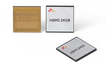
SK hynix announced today it has become the industry's first to develop 12-layer HBM3 product with a 24 gigabyte (GB) memory capacity, currently the largest in the industry, and said customers' performance evaluation of samples is underway. HBM (High Bandwidth Memory): A high-value, high-performance memory that vertically interconnects multiple DRAM chips and dramatically increases data processing speed in comparison to traditional DRAM products. HBM3 is the 4th generation product, succeeding the previous generations HBM, HBM2 and HBM2E
"The company succeeded in developing the 24 GB package product that increased the memory capacity by 50% from the previous product, following the mass production of the world's first HBM3 in June last year," SK hynix said. "We will be able to supply the new products to the market from the second half of the year, in line with growing demand for premium memory products driven by the AI-powered chatbot industry." SK hynix engineers improved process efficiency and performance stability by applying Advanced Mass Reflow Molded Underfill (MR-MUF)# technology to the latest product, while Through Silicon Via (TSV)## technology reduced the thickness of a single DRAM chip by 40%, achieving the same stack height level as the 16 GB product.
# MR-MUF (Mass Reflow Molded Underfill): A method of placing multiple chips on the lower substrate and bonding them at once through reflow, and then simultaneously filling the gap between the chips or between the chip and the substrate with a mold material.
## TSV (Through Silicon Via): An interconnecting technology used in advanced packaging that links the upper and lower chips with electrode that vertically passes through thousands of fine holes on DRAM chips. SK hynix's HBM3 that integrated this technology can process up to 819 GB per second, meaning that 163 FHD (Full-HD) movies can be transmitted in a single second
The HBM, first developed by SK hynix in 2013, has drawn broad attention from the memory chip industry for its crucial role in implementing generative AI that operates in high-performance computing (HPC) systems.
The latest HBM3 standard, in particular, is considered the optimal product for rapid processing of large volumes of data, and therefore its adoption by major global tech companies is on the rise.
SK hynix has provided samples of its 24 GB HBM3 product to multiple customers that have expressed great expectation for the latest product, while the performance evaluation of the product is in progress.
"SK hynix was able to continuously develop a series of ultra-high speed and high capacity HBM products through its leading technologies used in the back-end process," said Sang Hoo Hong, Head of Package & Test at SK hynix. "The company plans to complete mass production preparation for the new product within the first half of the year to further solidify its leadership in cutting-edge DRAM market in the era of AI."
View at TechPowerUp Main Site
"The company succeeded in developing the 24 GB package product that increased the memory capacity by 50% from the previous product, following the mass production of the world's first HBM3 in June last year," SK hynix said. "We will be able to supply the new products to the market from the second half of the year, in line with growing demand for premium memory products driven by the AI-powered chatbot industry." SK hynix engineers improved process efficiency and performance stability by applying Advanced Mass Reflow Molded Underfill (MR-MUF)# technology to the latest product, while Through Silicon Via (TSV)## technology reduced the thickness of a single DRAM chip by 40%, achieving the same stack height level as the 16 GB product.

# MR-MUF (Mass Reflow Molded Underfill): A method of placing multiple chips on the lower substrate and bonding them at once through reflow, and then simultaneously filling the gap between the chips or between the chip and the substrate with a mold material.
## TSV (Through Silicon Via): An interconnecting technology used in advanced packaging that links the upper and lower chips with electrode that vertically passes through thousands of fine holes on DRAM chips. SK hynix's HBM3 that integrated this technology can process up to 819 GB per second, meaning that 163 FHD (Full-HD) movies can be transmitted in a single second
The HBM, first developed by SK hynix in 2013, has drawn broad attention from the memory chip industry for its crucial role in implementing generative AI that operates in high-performance computing (HPC) systems.
The latest HBM3 standard, in particular, is considered the optimal product for rapid processing of large volumes of data, and therefore its adoption by major global tech companies is on the rise.
SK hynix has provided samples of its 24 GB HBM3 product to multiple customers that have expressed great expectation for the latest product, while the performance evaluation of the product is in progress.
"SK hynix was able to continuously develop a series of ultra-high speed and high capacity HBM products through its leading technologies used in the back-end process," said Sang Hoo Hong, Head of Package & Test at SK hynix. "The company plans to complete mass production preparation for the new product within the first half of the year to further solidify its leadership in cutting-edge DRAM market in the era of AI."
View at TechPowerUp Main Site


