• Welcome to TechPowerUp Forums, Guest! Please check out our forum guidelines for info related to our community.
  • The forums have been upgraded with support for dark mode. By default it will follow the setting on your system/browser. You may override it by scrolling to the end of the page and clicking the gears icon.

Samsung Claims 60-70% Yields for its 3 nm Node

btarunr

Editor & Senior Moderator
Staff member
Joined
Oct 9, 2007
Messages
47,857 (7.38/day)
Location
Dublin, Ireland
System Name RBMK-1000
Processor AMD Ryzen 7 5700G
Motherboard Gigabyte B550 AORUS Elite V2
Cooling DeepCool Gammax L240 V2
Memory 2x 16GB DDR4-3200
Video Card(s) Galax RTX 4070 Ti EX
Storage Samsung 990 1TB
Display(s) BenQ 1440p 60 Hz 27-inch
Case Corsair Carbide 100R
Audio Device(s) ASUS SupremeFX S1220A
Power Supply Cooler Master MWE Gold 650W
Mouse ASUS ROG Strix Impact
Keyboard Gamdias Hermes E2
Software Windows 11 Pro
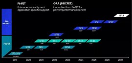
Samsung Electronics is engaged in stiff competition with TSMC for chip manufacturing orders for 3 nm, its first semiconductor foundry node to implement GAA-FET technology, after nearly a decade of FinFET-based nodes. SF3, a 3 nm GAA-FET node, enters mass-production later this year. Samsung is claiming wafer yields in the range of 60-70% in the development phases of the node. This number is crucial to attract customers as they base their wafer orders squarely on yields first, and cost-per-wafer next.

Samsung is trying to rebuild confidence among chip designers after the 2022 controversy over its engineering "fabricating" yield numbers to customers to win their business. Samsung also stated that with 2023-2024 being dominated by 3 nm-class nodes, namely SF3 (3GAP), and its refinement the SF3P (3GAP+), the company will begin introducing its 2 nm class nodes in 2025-2026. Samsung's current customers for its 3 nm node include unnamed HPC processor designer, and a mobile AP (application processor) designer.


View at TechPowerUp Main Site | Source
 
Is 60-70% yield normal in the Development Phase of a node?
 
Is 60-70% yield normal in the Development Phase of a node?
That's often at the point where they start production as far as I'm aware, with the expectation to improve from there. However, the issue is when things don't improve from there, then it gets very expensive for the foundry. TSMC was reported somewhere between 60 and 80%, which is a bit better, but also not as clear as to where in the span they might've been.
On top of that, it matters what type of chip it is, as smaller chips tend to have better yield rates than larger chips, since the defects are spread out across the entire silicon wafer. If you're lucky, the defects end up causing minimum issues, if you're unlucky, most of a wafer is unusable.
 
Last edited:
Semi-related, I'm also wondering if the last-level cache of today's processors is designed with manufacturing defects in mind, so it can operate when there's a small number of defects on it.
 
Semi-related, I'm also wondering if the last-level cache of today's processors is designed with manufacturing defects in mind, so it can operate when there's a small number of defects on it.
Caches are typically defect resistant due to some redundancy. The yield of a Ryzen chiplet is even higher than the naive calculation would indicate.
 
Caches are typically defect resistant due to some redundancy. The yield of a Ryzen chiplet is even higher than the naive calculation would indicate.
Do you have any sources for that? That is my assumption too, but I don't think there's redundancy in the form of additional cache lines (like Zen having 32.01 MiB total and 32 usable). Rather, the defective cache lines are just tagged as such and not used, which doesn't affect the operation of the rest of them (so there's 32 MiB total and 31.99 usable).
 
Do you have any sources for that? That is my assumption too, but I don't think there's redundancy in the form of additional cache lines (like Zen having 32.01 MiB total and 32 usable). Rather, the defective cache lines are just tagged as such and not used, which doesn't affect the operation of the rest of them (so there's 32 MiB total and 31.99 usable).
Sadly, my sources are for older processors and don't pertain to any that are current. Of course, given the high yield of these very small chiplets, at least AMD might have opted to forgo redundancy for the small savings in area.
 
Last edited:
Is Samsung making anything interesting at the moment?
I know the do nand and ram anything other than their own exynos?
 
So it's basically at most 40%. Which is on pair with Intel, or TSMC....
 
Back
Top