TheLostSwede
News Editor
- Joined
- Nov 11, 2004
- Messages
- 18,937 (2.51/day)
- Location
- Sweden
| System Name | Overlord Mk MLI |
|---|---|
| Processor | AMD Ryzen 7 7800X3D |
| Motherboard | Gigabyte X670E Aorus Master |
| Cooling | Noctua NH-D15 SE with offsets |
| Memory | 32GB Team T-Create Expert DDR5 6000 MHz @ CL30-34-34-68 |
| Video Card(s) | Gainward GeForce RTX 4080 Phantom GS |
| Storage | 1TB Solidigm P44 Pro, 2 TB Corsair MP600 Pro, 2TB Kingston KC3000 |
| Display(s) | Acer XV272K LVbmiipruzx 4K@160Hz |
| Case | Fractal Design Torrent Compact |
| Audio Device(s) | Corsair Virtuoso SE |
| Power Supply | be quiet! Pure Power 12 M 850 W |
| Mouse | Logitech G502 Lightspeed |
| Keyboard | Corsair K70 Max |
| Software | Windows 10 Pro |
| Benchmark Scores | https://valid.x86.fr/yfsd9w |
NEO Semiconductor, a leading developer of innovative technologies for 3D NAND flash and DRAM memory, today announced the launch of its ground-breaking technology, 3D X-DRAM. This development is the world's first 3D NAND-like DRAM cell array that is targeted to solve DRAM's capacity bottleneck and replace the entire 2D DRAM market. Relevant patent applications were published with the United States Patent Application Publication on April 6, 2023.
"3D X-DRAM will be the absolute future growth driver for the Semiconductor industry," said Andy Hsu, Founder and CEO of NEO Semiconductor and an accomplished technology inventor with more than 120 U.S. patents. "Today I can say with confidence that Neo is becoming a clear leader in the 3D DRAM market. Our invention, compared to the other solutions in the market today, is very simple and less expensive to manufacture and scale. The industry can expect to achieve 8X density and capacity improvements per decade with our 3D X-DRAM."
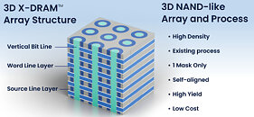

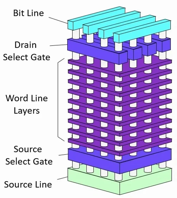
NEO Semiconductor's 3D X-DRAM is a first-of-its-kind 3D NAND-like DRAM cell array structure based on capacitor-less floating body cell technology. It can be manufactured using today's 3D NAND-like process and only needs one mask to define the bit line holes and form the cell structure inside the holes. This cell structure simplifies the process steps and provides a high-speed, high-density, low-cost, and high-yield solution. Based on Neo's estimates, 3D X-DRAM technology can achieve 128 Gb density with 230 layers, which is 8 times today's DRAM density.
An industry-wide effort is underway to bring 3D to DRAM. Adopting 3D X-DRAM involves leveraging the current mature 3D NAND process only, unlike many of the alternatives for moving DRAM to 3D proposed by academic papers and researched by the memory industry. Without 3D X-DRAM, the industry faces waiting potential decades, navigating inevitable manufacturing disruptions, and mitigating unacceptable yield and cost challenges. 3D X-DRAM is the necessary solution to address the increase in demand for high-performance and high-capacity memory semiconductors driven by the next wave of artificial intelligence (AI) applications such as ChatGPT.
"Evolving from 2D to 3D architectures has introduced compelling and extremely valuable benefits to NAND flash, so achieving a similar evolution for DRAM is highly desirable industry-wide," said Jay Kramer, President of Network Storage Advisors. "NEO Semiconductor's innovative 3D X-DRAM allows the memory industry to leverage current technologies, nodes and processes for enhancing DRAM products with NAND-like 3D architectures."
View at TechPowerUp Main Site | Source
"3D X-DRAM will be the absolute future growth driver for the Semiconductor industry," said Andy Hsu, Founder and CEO of NEO Semiconductor and an accomplished technology inventor with more than 120 U.S. patents. "Today I can say with confidence that Neo is becoming a clear leader in the 3D DRAM market. Our invention, compared to the other solutions in the market today, is very simple and less expensive to manufacture and scale. The industry can expect to achieve 8X density and capacity improvements per decade with our 3D X-DRAM."


NEO Semiconductor's 3D X-DRAM is a first-of-its-kind 3D NAND-like DRAM cell array structure based on capacitor-less floating body cell technology. It can be manufactured using today's 3D NAND-like process and only needs one mask to define the bit line holes and form the cell structure inside the holes. This cell structure simplifies the process steps and provides a high-speed, high-density, low-cost, and high-yield solution. Based on Neo's estimates, 3D X-DRAM technology can achieve 128 Gb density with 230 layers, which is 8 times today's DRAM density.
An industry-wide effort is underway to bring 3D to DRAM. Adopting 3D X-DRAM involves leveraging the current mature 3D NAND process only, unlike many of the alternatives for moving DRAM to 3D proposed by academic papers and researched by the memory industry. Without 3D X-DRAM, the industry faces waiting potential decades, navigating inevitable manufacturing disruptions, and mitigating unacceptable yield and cost challenges. 3D X-DRAM is the necessary solution to address the increase in demand for high-performance and high-capacity memory semiconductors driven by the next wave of artificial intelligence (AI) applications such as ChatGPT.
"Evolving from 2D to 3D architectures has introduced compelling and extremely valuable benefits to NAND flash, so achieving a similar evolution for DRAM is highly desirable industry-wide," said Jay Kramer, President of Network Storage Advisors. "NEO Semiconductor's innovative 3D X-DRAM allows the memory industry to leverage current technologies, nodes and processes for enhancing DRAM products with NAND-like 3D architectures."
View at TechPowerUp Main Site | Source