• Welcome to TechPowerUp Forums, Guest! Please check out our forum guidelines for info related to our community.
  • The forums have been upgraded with support for dark mode. By default it will follow the setting on your system/browser. You may override it by scrolling to the end of the page and clicking the gears icon.

Intel Lunar Lake-MX SoC with On-Package LPDDR5X Memory Detailed

btarunr

Editor & Senior Moderator
Staff member
Joined
Oct 9, 2007
Messages
47,695 (7.42/day)
Location
Dublin, Ireland
System Name RBMK-1000
Processor AMD Ryzen 7 5700G
Motherboard Gigabyte B550 AORUS Elite V2
Cooling DeepCool Gammax L240 V2
Memory 2x 16GB DDR4-3200
Video Card(s) Galax RTX 4070 Ti EX
Storage Samsung 990 1TB
Display(s) BenQ 1440p 60 Hz 27-inch
Case Corsair Carbide 100R
Audio Device(s) ASUS SupremeFX S1220A
Power Supply Cooler Master MWE Gold 650W
Mouse ASUS ROG Strix Impact
Keyboard Gamdias Hermes E2
Software Windows 11 Pro
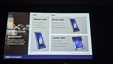
With the reality of high performance Arm processors from Apple and Qualcomm threatening Intel's market share in the client computing space, Intel is working on learner more PCB-efficient client SoCs that can take the fight to them, while holding onto the foundations of x86. The first such form-factor of processors are dubbed -MX. These are essentially -U segment processors with memory on package, to minimize PCB footprint. Intel has fully integrated the PCH into the processor chip with "Meteor Lake," with PCH functions scattered across the SoC and I/O tiles of the processor. An SoC package with dimensions similar to those of -UP4 packages meant for ultrabooks, can now cram main memory, so the PCBs of next-generation notebooks can be further compacted.

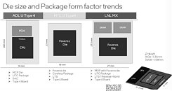
Intel had recently shown Meteor Lake-MX packages to the press as a packaging technology demonstration in its Arizona facility. It's unclear whether this could release as actual products, but in a leaked company presentation, confirmed that its first commercial outing will be with Lunar Lake-MX. The current "Alder Lake-UP4" package measures 19 mm x 28.5 mm, and is a classic multi-chip module that combines a monolithic "Alder Lake" SoC die with a PCH die. The "Meteor Lake-UP4" package measures 19 mm x 23 mm, and is a chiplet-based processor, with a Foveros base tile that holds the Compute (CPU cores), Graphics (iGPU), SoC and I/O (platform core-logic) tiles. The "Lunar Lake-MX" package is slightly larger than its -UP4 predecessors, measuring 27 mm x 27.5 mm, but completely frees up space on the PCB for memory.


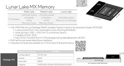
The "Lunar Lake-MX" package features a Foveros base tile, just like "Meteor Lake-UP4," but with two LPDDR5X memory chips on package. Depending on the processor model, the memory sizes on offer will be either 16 GB or 32 GB, across a 160-bit dual-channel (4x sub-channel) interface. Memory speeds on offer will be as high as LP5X-8533. Intel is innovating what it calls a "memory side cache," which is an 8 MB fast SRAM cache located somewhere along the memory I/O.

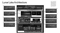
The "Lunar Lake" microarchitecture is expected to see Intel reorganize the various components of the SoC across the tiles. There is expected to be one large logic-heavy tile called the "CPU tile," and a smaller platform core-logic heavy tile called the "SoC tile." With Lunar Lake, Intel Foundry Services (IFS) is expected to debut the company Intel 18A foundry node, which offers transistor densities and power/thermal characteristics comparable to 2 nm-class nodes by TSMC. From the looks of it, the entire CPU tile will be built on the TSMC N3B (3 nm) foundry node.


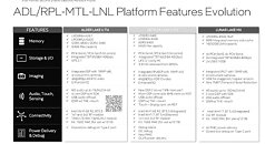
The CPU tile contains the compute complex along the high bandwidth North Fabric. The key components here are the Performance Compute cores, the Low-Power core clusters; the next-generation NPU which accelerates AI, the iGPU based on the Xe2 "Battlemage" graphics architecture, and the LPDDR5X memory controllers. There are other minor bandwidth-hungry components, such as the IPU (image processing), and media engine (video accelerators). The SoC die is now back to being a glorified PCH, with the various platform interfaces, PCIe, USB, and Thunderbolt I/O.

The compute muscle of "Lunar Lake-MX" will see a CPU with a 4P+4E configuration, with a very high degree of interoperability integration with the OS. The performance cores (P-cores) are codenamed "Lion Cove," and will be three generations ahead of the current "Raptor Cove," which means three consecutive cycles of IPC uplifts. The efficiency cores (E-cores) are codenamed "Skymont" and will be two generations ahead of the current "Gracemont." The upcoming "Crestmont" E-core architecture will be deployed on "Meteor Lake" and "Arrow Lake."

The graphics muscle is care of the Xe²-LPG graphics architecture, which draws from Intel's next-generation gaming graphics architecture codenamed "Battlemage." The iGPU on the "Lunar Lake-MX" package has 8 Xe cores worth 64 16-wide vector engines, full DirectX 12 Ultimate API feature-set, and hardware support for Intel's next systolic AI superscaling technology.

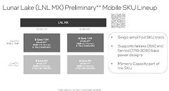
We are still far away from actual processor model numbers and SKUs, but Intel has drawn up some draft SKU segmentation for "Lunar Lake-MX." It sees 32 GB and 16 GB variants of Core 7 SKUs with 4P+4E CPUs and 8 Xe cores; and 32 GB and 16 GB variants of Core 5 SKUs with 4P+4E CPUs, and 7 Xe cores. Intel is targeting power envelopes as low as 8 W, for completely fanless devices, going all the way up to 30 W for high performance variants. The company aims for "Lunar Lake-MX" to compete in the same device category as the 2025 successors of Apple M3.

View at TechPowerUp Main Site | Source
 
“From the looks of it, the entire CPU tile will be built on the TSMC N3B (3 nm) foundry node.”

Intel continues to eschew its own fab processes for third party fabs, first with GPUs now with CPUs.

Best case scenario, Intel 4 and Intel 3 processes are not doing well. Worst case scenario, Intel is trying to deny fab capacity to TSMC clients like AMD. And before I get trashed, ask yourself one question, why does Intel need to fab anything, ANYTHING AT ALL, at TSMC?
Many reasons
1. Less TSMC waffers for the concurrency - AMD and Apple
2. Selling their own trash nodes sponsored by the tax payers to third parties and buying superior nodes with the money from TSMC
3. No longer delayed next gen nodes for their products
 
“From the looks of it, the entire CPU tile will be built on the TSMC N3B (3 nm) foundry node.”

Intel continues to eschew its own fab processes for third party fabs, first with GPUs now with CPUs.

Best case scenario, Intel 4 and Intel 3 processes are not doing well. Worst case scenario, Intel is trying to deny fab capacity to TSMC clients like AMD. And before I get trashed, ask yourself one question, why does Intel need to fab anything, ANYTHING AT ALL, at TSMC?
And the sentence before "With Lunar Lake, Intel Foundry Services (IFS) is expected to debut the company Intel 18A foundry node, which offers transistor densities and power/thermal characteristics comparable to 2 nm-class nodes by TSMC." But this is probably wishful thinking. I doubt Intel would abandon their fabs only to block others from TSMC. In the long run this will give TSMC profits to build more fabs so they can serve both Intel and AMD, but both after Apple and then Samsung has its own fabs. The only way for x86 to survive is if Intel to catch up with TSMC.

Many reasons
1. Less TSMC waffers for the concurrency - AMD and Apple
2. Selling their own trash nodes sponsored by the tax payers to third parties and buying superior nodes with the money from TSMC
3. No longer delayed next gen nodes for their products
Why would any third party buy from Intel if they can from TSMC.
TSMC can invest Intel money to build more fabs.
Intel will fabs soon will be competing with GloFo not with TSMC and Samsung.
 
These look very good for Surface and ultraportables, at least on paper.

Going with TSMC, instead of keep hitting their head on their manufacturing wall expecting the result to be less pain and humiliation, is the logical decision.
 
“From the looks of it, the entire CPU tile will be built on the TSMC N3B (3 nm) foundry node.”

Intel continues to eschew its own fab processes for third party fabs, first with GPUs now with CPUs.

Best case scenario, Intel 4 and Intel 3 processes are not doing well. Worst case scenario, Intel is trying to deny fab capacity to TSMC clients like AMD. And before I get trashed, ask yourself one question, why does Intel need to fab anything, ANYTHING AT ALL, at TSMC?
Looking at slide from 2022, Intel 3 or even 20A was never planned for Lunar lake
1700485695799.png
 
why does Intel need to fab anything, ANYTHING AT ALL, at TSMC?
So they can have those "five new nodes in four years" - which includes TSMC's nodes.
 
Intel will fabs soon will be competing with GloFo not with TSMC and Samsung.
The US govt basically stated they wont let that happen.
 
I'd like to see how well they can maintain performance with the constraint of a low TDP. Unfortunately, TDP on intel CPUs is always a fraud, 8-9w = 20-25w.
 
This is just my opinion, but i think the main reason Intel use TSMC is not because they are abandoning their own fab business, but more because they don't have enough capacity to produce enough leading edge to fill the market.

They probably made good step on newer nodes, but they are still one of the market giant and they have to produce a lot of chip to fill the market. They are now just moving to chiplet and they still produce a lot of large monolithic chips that is probably affecting their yield a lot.

They probably have to go to TSMC to not lose market share.

We will see once they embrace the chiplets if they still depend a lot on TSMC. There might also be some industrial espionage going on too.
 
Finally, on-package DRAM for Intel laptops. Tired of reading nonsense that "Intel & AMD are just a few nodes behind honestly," when Apple was a leader in DRAM packaging.

Just 4 years after Apple's M1 (2020)
Just 6 years after the iPad A12X (2018)
Just 9 years after PoP DRAM in smartphones (2015).

I wonder when AMD & Qualcomm might join. How long can you ignore key power savings?

Apple started off the presentation with a showcase of the packaging, there the M1 Pro is shown to continue to feature very custom packaging, including the still unique characteristic that Apple is packaging the SoC die along with the memory dies on a single organic PCB, which comes in contrast to other traditional chips such as from AMD or Intel which feature the DRAM dies either in DIMM slots, or soldered onto the motherboard. Apple’s approach here likely improves power efficiency by a notable amount.

If we're soldering RAM (and virtually everyone is in efficiency-focused laptops), then might as well go all the way.
 
As long as this is for ultraportables like surfaces, and tablets, thats fine.
If they are wanting to generalise this for all laptops then no.
Id like to be able to upgrade/change dram in laptops...
 
Finally, on-package DRAM for Intel laptops. Tired of reading nonsense that "Intel & AMD are just a few nodes behind honestly," when Apple was a leader in DRAM packaging.

Just 4 years after Apple's M1 (2020)
Just 6 years after the iPad A12X (2018)
Just 9 years after PoP DRAM in smartphones (2015).

I wonder when AMD & Qualcomm might join. How long can you ignore key power savings?


If we're soldering RAM (and virtually everyone is in efficiency-focused laptops), then might as well go all the way.

Why do you care about on-package ram? Apple uses it because the latency otherwise would be huge, they are already at comparable levels to AMD. Any worse would absolutely affect the performance of their M series chips
 
This is just my opinion, but i think the main reason Intel use TSMC is not because they are abandoning their own fab business, but more because they don't have enough capacity to produce enough leading edge to fill the market.

They probably made good step on newer nodes, but they are still one of the market giant and they have to produce a lot of chip to fill the market. They are now just moving to chiplet and they still produce a lot of large monolithic chips that is probably affecting their yield a lot.

They probably have to go to TSMC to not lose market share.

We will see once they embrace the chiplets if they still depend a lot on TSMC. There might also be some industrial espionage going on too.
I might agree with you except for IFS. If Intel is capacity constrained why are they trying to sell advanced node capacity to other companies?
 
The US govt basically stated they wont let that happen.
The US government can give Intel money and even suppress Intel's competition, but they can't make Intel succeed. You can lead a horse to water but you can't make it drink.

[Why] does Intel need to fab anything, ANYTHING AT ALL, at TSMC?
One aspect might be specialization of the nodes. Intel 4 is frequency-optimized, so it's the logical choice for Meteor Lake's CPU tile. Intel 3 can be density-optimized, making it the logical choice for the GPU and SoC tiles, but Intel 3 isn't ready and TSMC N5 and N6 are, and as it happens these are being used for the GPU and SoC tiles of Meteor Lake. Intel 20A will be frequency-optimized and Intel 18A will be able to be density-optimized.

I'm not sure why Arrow Lake would have TSMC parts. It seems to me that an Intel 20A CPU tile with Intel 3 GPU and SoC tiles ought to do quite well if 3 and 20A can be produced in enough quantity. And if Lunar Lake has access to all these and Intel 18A, then there oughtn't be a need for TSMC in that product.
 
8MB on the "northbridge", but no word on how much cache there'll be on the iGPU/iNPU.
Considering how memory latency was apparently Archmage's biggest problem, I wonder if Intel spent enough time and effort fixing this.
 
The US government can give Intel money and even suppress Intel's competition, but they can't make Intel succeed. You can lead a horse to water but you can't make it drink.


One aspect might be specialization of the nodes. Intel 4 is frequency-optimized, so it's the logical choice for Meteor Lake's CPU tile. Intel 3 can be density-optimized, making it the logical choice for the GPU and SoC tiles, but Intel 3 isn't ready and TSMC N5 and N6 are, and as it happens these are being used for the GPU and SoC tiles of Meteor Lake. Intel 20A will be frequency-optimized and Intel 18A will be able to be density-optimized.

I'm not sure why Arrow Lake would have TSMC parts. It seems to me that an Intel 20A CPU tile with Intel 3 GPU and SoC tiles ought to do quite well if 3 and 20A can be produced in enough quantity. And if Lunar Lake has access to all these and Intel 18A, then there oughtn't be a need for TSMC in that product.
I doubt Intel 4 is frequency optimized. If that was the case, they would have used it for the desktop CPUs. It is energy efficiency optimized process. They don't even bother to use Intel 3 in desktop CPUs so it won't be frequency optimized either. 20A is supposed to be frequency optimized as it will be used for desktop Arrow Lake. But it might have changed.
 
I doubt Intel 4 is frequency optimized. If that was the case, they would have used it for the desktop CPUs. It is energy efficiency optimized process. They don't even bother to use Intel 3 in desktop CPUs so it won't be frequency optimized either. 20A is supposed to be frequency optimized as it will be used for desktop Arrow Lake. But it might have changed.
According to Tom's hardware, "Compared to Intel 4, Intel 3 promises an 18% higher performance per watt efficiency, denser high-performance library, reduced via resistance, and increased intrinsic drive current." https://www.tomshardware.com/news/intel-3nm-class-node-meets-defect-density-and-performance-targets

So IFS doesn't claim that Intel 3 offers any frequency-related advantages over Intel 4. Instead its advantages are density and power improvements. I know Intel 4 is going only to mobile processors which strongly implies that it can't reach high frequencies, but the same was true of Intel 7/10ESF/10SF/10nm+/10nm when it was released to mobile-only as Tiger Lake and before that U-series-only as Ice Lake, and 14nm before it first came to Broadwell which never targetted high-performance desktop. Intel 4 might achieve higher frequencies later, around the time Intel claims Arrow Lake will be coming to desktop on Intel 20A.

But you're probably right, Intel 4 isn't really frequency-optimized just yet, but it seems to be missing a lot of high-density features that would be very useful to a GPU or a SoC.
Intel has promised a lot of things. Like here https://www.techpowerup.com/250394/...ck-on-track-2x-transistor-densities-over-10nm
7 nm EUV being on track would mean a qualitative rollout within or toward the end of 2019, and mass-production of chips slated for 2020-21.
And it is now on track for late 2023.
I doubt Intel 3 is actually what used to be 5nm, it is rather 7nm++ while Intel 4 is 7nm+ while initial 7nm was so bad it wasn't production worth. I rather think 20A will be 5nn and 18A 5nm+.
And finally if Intel 3 will have "denser high-performance library" than I understand thi as it will offer higher performance than Intel 4. I might be wrong with my interpretation.

This is just my opinion, but i think the main reason Intel use TSMC is not because they are abandoning their own fab business, but more because they don't have enough capacity to produce enough leading edge to fill the market.

They probably made good step on newer nodes, but they are still one of the market giant and they have to produce a lot of chip to fill the market. They are now just moving to chiplet and they still produce a lot of large monolithic chips that is probably affecting their yield a lot.

They probably have to go to TSMC to not lose market share.

We will see once they embrace the chiplets if they still depend a lot on TSMC. There might also be some industrial espionage going on too.
but they are already transitioning from producing large monolithic CPUs in 10nm to producing only CPU tile in Intel 4 while the rest of tiles at TSMC and they are building 4 new fabs. At least 2 of these fabs are expected to be finished in next year and start producing 20A CPU tiles even with poor yields they should produce more CPU tiles than they are producing whole CPUs in Intel 7 now. If 4. 3 and 20A will be on time ind successful, they should have plenty of free capacity in 10/7nm fabs. Is it better to use them to produce for 3rd parties and produce their own at TSMC? I think it would be better to convert these fabs to 18A and produce their own CPUs.
 
Why do you care about on-package ram? Apple uses it because the latency otherwise would be huge, they are already at comparable levels to AMD. Any worse would absolutely affect the performance of their M series chips

Who told you Apple chose on-package DRAM for latency? :roll: I'd like the source of that nonsense.

Apple's, and Intel's, on-package DRAM is for power savings and space savings. Read AnandTech that I linked or the source article you're commenting under.

On-Package LPDDR5x delivering higher memory bandwidth at reduced footprint and power.

Intel attempted on-package DRAM in 2014, but never shipped, IIRC: unfortunately typical for Intel, but Intel will gladly explain the benefits of on-package DRAM to you:

Xnapper-2023-11-21-09.28.03.png
 
Last edited:
And before I get trashed, ask yourself one question, why does Intel need to fab anything, ANYTHING AT ALL, at TSMC?
Many reasons
1. Less TSMC waffers for the concurrency - AMD and Apple
2. Selling their own trash nodes sponsored by the tax payers to third parties and buying superior nodes with the money from TSMC
3. No longer delayed next gen nodes for their products
The pedestrian reasons as well - capacity, cost.
Intel manufacturing something at TSMC is not new. What is new is Intel having state of the art CPUs manufactured at TSMC.
 
As long as this is for ultraportables like surfaces, and tablets, thats fine.
If they are wanting to generalise this for all laptops then no.
Id like to be able to upgrade/change dram in laptops...
... or, at the very least, have some choice when ordering a laptop. With RAM on processor package you don't even get that.
 
Back
Top