T0@st
News Editor
- Joined
- Mar 7, 2023
- Messages
- 3,113 (3.91/day)
- Location
- South East, UK
| System Name | The TPU Typewriter |
|---|---|
| Processor | AMD Ryzen 5 5600 (non-X) |
| Motherboard | GIGABYTE B550M DS3H Micro ATX |
| Cooling | DeepCool AS500 |
| Memory | Kingston Fury Renegade RGB 32 GB (2 x 16 GB) DDR4-3600 CL16 |
| Video Card(s) | PowerColor Radeon RX 7800 XT 16 GB Hellhound OC |
| Storage | Samsung 980 Pro 1 TB M.2-2280 PCIe 4.0 X4 NVME SSD |
| Display(s) | Lenovo Legion Y27q-20 27" QHD IPS monitor |
| Case | GameMax Spark M-ATX (re-badged Jonsbo D30) |
| Audio Device(s) | FiiO K7 Desktop DAC/Amp + Philips Fidelio X3 headphones, or ARTTI T10 Planar IEMs |
| Power Supply | ADATA XPG CORE Reactor 650 W 80+ Gold ATX |
| Mouse | Roccat Kone Pro Air |
| Keyboard | Cooler Master MasterKeys Pro L |
| Software | Windows 10 64-bit Home Edition |
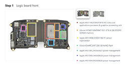
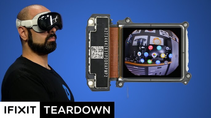
iFixit has finally posted photos of the Apple Vision Pro's inner bits, following on from the release of a video teardown (uploaded last week)—the American e-commerce and how-to website spent plenty of hours exploring the expensive mixed reality headset's "creepy" features, before breaking seals and deconstructing the device's highly complex interior. The iFixit teardown team have often complained about Apple computer products being notoriously difficult to deal with—the Vision Pro is no exception, but they eventually managed to isolate the headset's logic board. The onboard M2 octa-core chipset is identified as a APL1109/339S01081E part, while its assistant R1 sensor co-processor sports an APL1W08/339S01186 identifier. Micron has supplied 8 GB of LPDDR5 SDRAM memory (MT62F1G64D8WT-031 XT), and Kioxia has Apple covered with its K5A4RC2097 256 GB NAND flash.
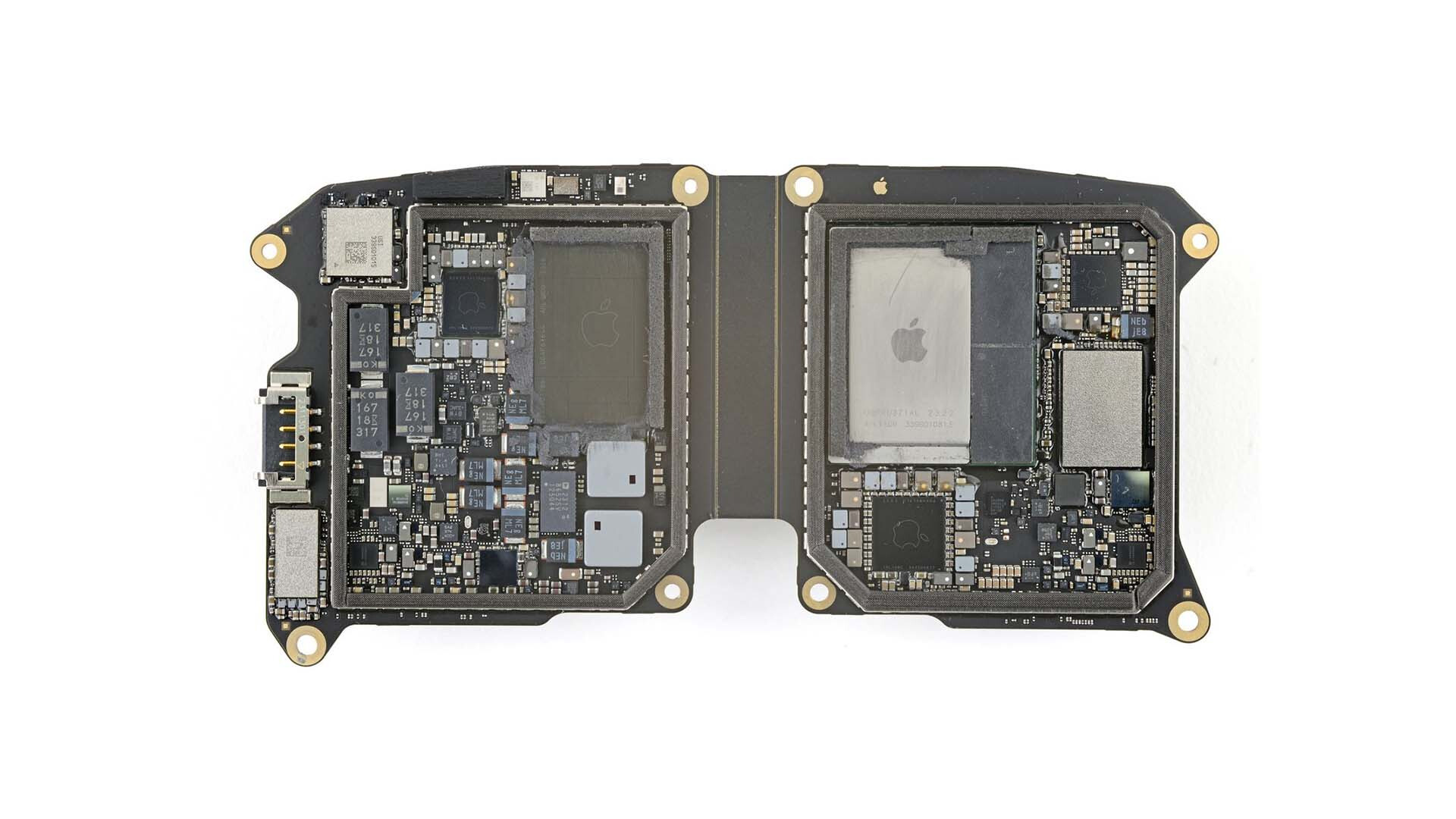
Tech experts have spent time poring over iFixit's latest set of snaps, as laid out in their teardown guide—one such enthusiast, Yining Karl Li, posted an intriguing Apple Vision Pro Logic Board observation to social media: "There's this interesting shot of the main logic board (in Step 1). The R1 chip (in the red box) has interesting lines all over it dividing the surface into sub-boxes. Is the R1 chip using a chiplet design?" A small debate erupted from this quick inspection—one commenter believes that the co-processor is not all that fancy: "(it is) likely sporting low-latency fan-out memory," citing the presence of very faint horizontal and vertical lines. As pointed out by Wccftech, Li also presented a chiplet design example (for comparison purposes)—a close-up shot of Intel's Ponte Vecchio Xe-HPC GPU. The lines are a lot more pronounced on Team Blue's chip design.


Here is iFixit's "Vision Pro Teardown: Behind the Complex and Creepy Tech" video:
View at TechPowerUp Main Site | Source
Tech experts have spent time poring over iFixit's latest set of snaps, as laid out in their teardown guide—one such enthusiast, Yining Karl Li, posted an intriguing Apple Vision Pro Logic Board observation to social media: "There's this interesting shot of the main logic board (in Step 1). The R1 chip (in the red box) has interesting lines all over it dividing the surface into sub-boxes. Is the R1 chip using a chiplet design?" A small debate erupted from this quick inspection—one commenter believes that the co-processor is not all that fancy: "(it is) likely sporting low-latency fan-out memory," citing the presence of very faint horizontal and vertical lines. As pointed out by Wccftech, Li also presented a chiplet design example (for comparison purposes)—a close-up shot of Intel's Ponte Vecchio Xe-HPC GPU. The lines are a lot more pronounced on Team Blue's chip design.

Here is iFixit's "Vision Pro Teardown: Behind the Complex and Creepy Tech" video:
View at TechPowerUp Main Site | Source
