• Welcome to TechPowerUp Forums, Guest! Please check out our forum guidelines for info related to our community.

JEDEC Updates DDR5 Specification for Increased Security Against Rowhammer Attacks, New DDR5-8800 Reference Speed

btarunr

Editor & Senior Moderator
Staff member
Joined
Oct 9, 2007
Messages
47,670 (7.43/day)
Location
Dublin, Ireland
System Name RBMK-1000
Processor AMD Ryzen 7 5700G
Motherboard Gigabyte B550 AORUS Elite V2
Cooling DeepCool Gammax L240 V2
Memory 2x 16GB DDR4-3200
Video Card(s) Galax RTX 4070 Ti EX
Storage Samsung 990 1TB
Display(s) BenQ 1440p 60 Hz 27-inch
Case Corsair Carbide 100R
Audio Device(s) ASUS SupremeFX S1220A
Power Supply Cooler Master MWE Gold 650W
Mouse ASUS ROG Strix Impact
Keyboard Gamdias Hermes E2
Software Windows 11 Pro
JEDEC Solid State Technology Association, the global leader in standards development for the microelectronics industry, today announced publication of the JESD79-5C DDR5 SDRAM standard. This important update to the JEDEC DDR5 SDRAM standard includes features designed to improve reliability and security and enhance performance in a wide range of applications from high-performance servers to emerging technologies such as AI and machine learning. JESD79-5C is now available for download from the JEDEC website.

JESD79-5C introduces an innovative solution to improve DRAM data integrity called Per-Row Activation Counting (PRAC). PRAC precisely counts DRAM activations on a wordline granularity. When PRAC-enabled DRAM detects an excessive number of activations, it alerts the system to pause traffic and to designate time for mitigative measures. These interrelated actions underpin PRAC's ability to provide a fundamentally accurate and predictable approach for addressing data integrity challenges through close coordination between the DRAM and the system.


Additional features offered in JESD79-5C DDR5 include:
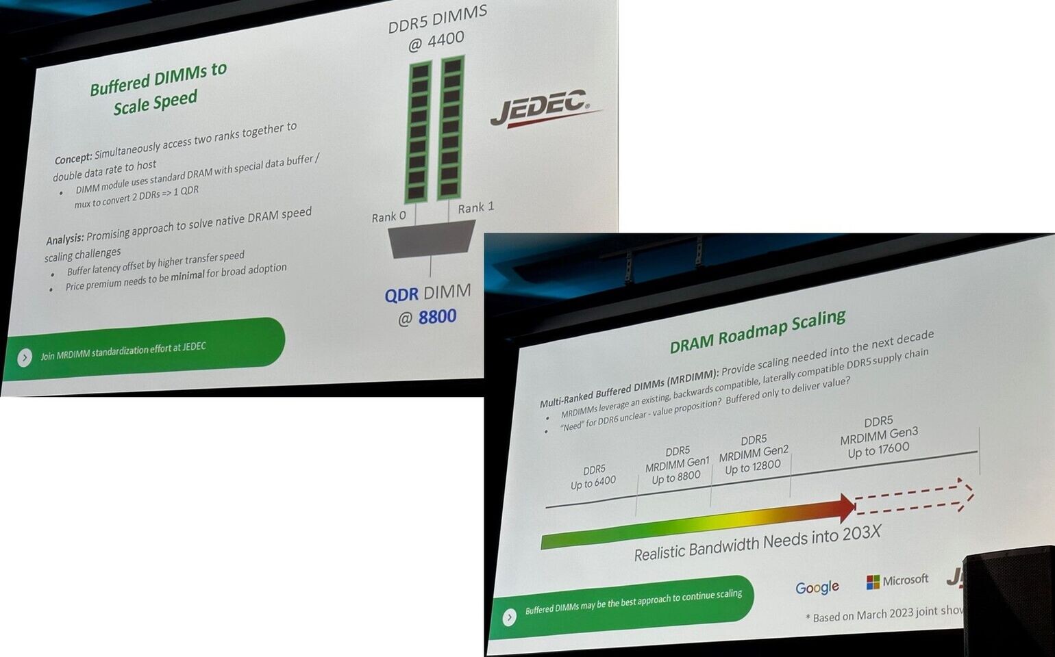
  • Expansion of timing parameters definition from 6800 Mbps to 8800 Mbps
  • Inclusion of DRAM core timings and Tx/Rx AC timings extended up to 8800 Mbps, compared to the previous version which supported only up to 6400 timing parameters and partial pieces up to 7200 DRAM core timings
  • Introduction of Self-Refresh Exit Clock Sync for I/O Training Optimization
  • Incorporation of DDP (Dual-Die Package) timings
  • Deprecation of PASR (Partial Array Self Refresh) to address security concerns
"I'm delighted to highlight the collaborative efforts of JEDEC's JC-42 Committee for Solid State Memory to advance the DDR5 standard," said Mian Quddus, JEDEC Board of Directors Chairman. He added, "Groundbreaking new features in JESD79-5C are intended to support ever-evolving industry demands for security, reliability and performance in a wide range of applications."

"The JC-42 Committee is pleased to unveil PRAC, a comprehensive solution to help ensure DRAM data integrity, as an integral component of the DDR5 update. Work is underway to incorporate this feature into other DRAM product families within JEDEC," noted Christopher Cox, JC-42 Committee Chair.

View at TechPowerUp Main Site
 
What are the timings on this new reference? Absolutely woeful, I would assume?
 
What are the timings on this new reference? Absolutely woeful, I would assume?
These are the A-grade timings.
1713862236687.png

 
@TheLostSwede
Yeah, not great for anything latency sensitive, so I guess client memory will stick with XMP/EXPO to tighten those up. I assume the new reference is mostly for server/datacenter platforms to increase bandwidth in those workloads when latency isn’t a concern?
 
@TheLostSwede There is something I don't understand about those numbers.
Why are the timings sometimes increases by 4 and sometimes only by 2, while each step is 400MT/s?
Are they arbitrarily lowering the timings just to stay within a certian latency limit?
 
I assume the new reference is mostly for server/datacenter platforms to increase bandwidth in those workloads when latency isn’t a concern?
Of course. Even with 8 or 12 or 16 channels, the bandwidth divided by the number of cores isn't great.

@TheLostSwede There is something I don't understand about those numbers.
Why are the timings sometimes increases by 4 and sometimes only by 2, while each step is 400MT/s?
Are they arbitrarily lowering the timings just to stay within a certian latency limit?
You can see it's always rounded to 14 nanoseconds. It could be a better approximation if odd number of cycles were possible (such as DDR5-6400 CL 45) but for some reason there are no odd latencies in DDR5, and they are rare in DDR4.

Also: that table has it wrong. (Which is not uncommon for Anandtech.) It should list CL timings for the A, B and C grades but instead, it lists CL timings for the A, A and A grades. The correct values would be around 14 ns, 16 ns and 18 ns, I suppose.
 
Last edited:
@TheLostSwede There is something I don't understand about those numbers.
Why are the timings sometimes increases by 4 and sometimes only by 2, while each step is 400MT/s?
Are they arbitrarily lowering the timings just to stay within a certian latency limit?
Look at the absolute latency figures. I presume JEDEC is trying to keep that at around 14.
That said, I don't know what the actual reason for that is.
 
There was some talk a year ago about multiplexed DIMMs, TPU too brought some news:


But I've seen no news about those recently. Are MRDIMM and MCRDIMM dead? Temporarily dead?
 
The big news here for me is the rowhammer security mitigations, really. Otherwise it's just more of the same JEDEC timings...

One does wonder what impact this'll have though, if any:

Deprecation of PASR (Partial Array Self Refresh) to address security concerns
 
Yeah, not great for anything latency sensitive, so I guess client memory will stick with XMP/EXPO to tighten those up. I assume the new reference is mostly for server/datacenter platforms to increase bandwidth in those workloads when latency isn’t a concern?
While there are some use cases where tighter timings have some advantages, it's usually just a few percent except for some edge cases, and most non-gaming workloads scale better with increased bandwidth anyways. Running overclocked memory does come at a cost too; system instability, wear and file corruption. It's a high price to pay for overpriced (mostly junk) memory, with minimal gain and major disadvantages.

Look at the absolute latency figures. I presume JEDEC is trying to keep that at around 14.
That said, I don't know what the actual reason for that is.
They optimize for power draw and reliability. Tightening the latency would require a lot more voltage.

I'm actually surprised to see them pushing DDR5 specs this much so quickly compared to the past generations, this will at least make up a little bit for the shortcomings of mainstream platforms having only two channels. I do wonder how long it will take Intel and AMD to have CPUs certified for these speeds, it's quite a jump up from their current support of 5600/5200 MHz respectively.
 
I don't know why jedec repeats the versions up to "4600" with DDR5. Doesn't make sense.
There's no reason generations shouldn't overlap in speeds. DDR2 and DDR3 did at 1066. DDR3 and DDR4 did at 1866 and 2133. Actually, if Wikipedia tables are complete, DDR4 and DDR5 meet at 3200 but don't overlap!

Also, while DDR5 modules below 4800 MT/s probably don't even exist, server processors support maximum speeds as low as 3600 in certain configurations, see this for an example. Maybe that's the reason JEDEC had to define lower speeds.
 
I'm mostly impressed that the manufacturers of Client Clock Drivers and Registering Clock Drivers are confident they can run up to 8800. Of course it may very well be a long time before we see native 8800 modules which aren't MCRDIMMs so perhaps it's not a gamble. JEDEC standards have always been about consistency and roughly 14ns has been used since DDR4 so I'm guessing it's something server platform holders have wanted.

JEDEC DDR4 specs went 2x over base during its lifetime and they're already 2.75x over base with DDR5 which I'm guessing is about enterprise compute density.
 
Back
Top