• Welcome to TechPowerUp Forums, Guest! Please check out our forum guidelines for info related to our community.
  • The forums have been upgraded with support for dark mode. By default it will follow the setting on your system/browser. You may override it by scrolling to the end of the page and clicking the gears icon.

AMD Granite Ridge and Strix Point Zen 5 Die-sizes and Transistor Counts Confirmed

btarunr

Editor & Senior Moderator
Staff member
Joined
Oct 9, 2007
Messages
47,849 (7.39/day)
Location
Dublin, Ireland
System Name RBMK-1000
Processor AMD Ryzen 7 5700G
Motherboard Gigabyte B550 AORUS Elite V2
Cooling DeepCool Gammax L240 V2
Memory 2x 16GB DDR4-3200
Video Card(s) Galax RTX 4070 Ti EX
Storage Samsung 990 1TB
Display(s) BenQ 1440p 60 Hz 27-inch
Case Corsair Carbide 100R
Audio Device(s) ASUS SupremeFX S1220A
Power Supply Cooler Master MWE Gold 650W
Mouse ASUS ROG Strix Impact
Keyboard Gamdias Hermes E2
Software Windows 11 Pro
AMD is about give the new "Zen 5" microarchitecture a near-simultaneous launch across both its client segments—desktop and mobile. The desktop front is held by the Ryzen 9000 "Granite Ridge" Socket AM5 processors; while Ryzen AI 300 "Strix Point" powers the company's crucial effort to capture Microsoft Copilot+ AI PC market share. We recently did a technical deep-dive on the two. HardwareLuxx.de scored two important bits of specs for both processors in its Q&A interaction with AMD—die sizes and transistor counts.

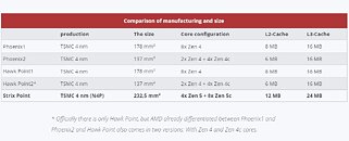
To begin with, "Strix Point" is a monolithic silicon, which is confirmed to be built on the TSMC N4P foundry node (4 nm). This is a slight upgrade over the N4 node that the company built its previous generation "Phoenix" and "Hawk Point" processors on. The "Strix Point" silicon measures 232.5 mm² in area, which is significantly larger than the 178 mm² of "Hawk Point" and "Phoenix." The added die area comes from there being 12 CPU cores instead of 8, and 16 iGPU compute units instead of 12; and a larger NPU. There are many other factors, such as the larger 24 MB CPU L3 cache; and the sizes of the "Zen 5" and "Zen 5c" cores themselves.


The "Granite Ridge" desktop processor is a chiplet-based processor, much like the Ryzen 7000 "Raphael." AMD is confirmed to be reusing the 6 nm client I/O die (cIOD) from "Raphael." This chip measures 122 mm², and packs 3.4 billion transistors. For reference, the cIOD of Ryzen 5000 "Vermeer" and Ryzen 3000 "Matisse" is built on the Global Foundries 12 nm node, measures a similar 125 mm², but with a much lower transistor count of 2.09 billion. The key contributor to the transistor count increase is the tiny iGPU that the Socket AM5 cIOD comes with. It may have just 1 workgroup processor (2 CU), but comes with the same display engines and media engines as the iGPU on APUs.

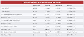
And now, onto the CPU complex dies (CCDs), the key area of silicon innovation for AMD desktop processors. The 8-core "Zen 5" CCD is codenamed "Eldora," and is built on the 4 nm foundry node. The HardwareLuxx.de report says that this the same N4P node as "Strix Point," but we've heard several other credible sources claiming that it is the more advanced N4X node, which favors high frequencies. The "Zen 5" CCD has a transistor count of 8.315 billion, which is a significant increase over the 6.5 billion of "Durango," the 8-core CCD based on "Zen 4," powering "Raphael."

What's most interesting is that this staggering 28% increase in transistor counts from the "Zen 4" Durango CCD to the "Zen 5" Eldora CCD comes at a die-area decrease of 0.5%. That's right, the "Zen 5" CCD measures 70.6 mm², whereas the "Zen 4" CCD is 71 mm². The "Zen 4" CCD is built on TSMC N5 (5 nm), which goes to show the leap in transistor densities achieved from the switch to N4P (or N4X).

A maxed out Ryzen 9 9950X processor hence has a total transistor count of 20.03 billion, while the single-CCD Ryzen 7 9700X has a transistor count of 11.715 billion.

AMD Ryzen 9000 series goes on sale from July 31, 2024.

View at TechPowerUp Main Site | Source
 
So Arrowlake will have a node advantage over Zen5?
 
So Arrowlake will have a node advantage over Zen5?

Only the igpu tile is on tsmc 4 whatever the core tile is still whatever intel wants to call it these days with thier own fabrication I believe.... 20A I think it's called but rumors are all the place with possible only the i9 series using it and the rest on tsmc so who knows at this point.

Would be kinda funny of the i7 on tsmc overclocks better and ends up more desirable lol but we still probably have 3-4 months to go.
I thought the Arrowlake CPU tile is on TSMC N3B
 
I thought the Arrowlake CPU tile is on TSMC N3B

Everything I've seen is intel 20A but could be wrong it's kinda a mess at intel when it comes to fabrication right now.

Some say only the high end will use 20A some say only the low end so it's really all over the place most leaks are from march or older.
 
More dense harder to cool, no surrounding silicon at same v height to diffuse.

Yeeeesh
 
What...I was expecting the dies to be larger than Zen 4 with more execution engines etc but it seems to be the same size with a substantial increase in density instead. But the added density doesn't seem to be affecting clocks so maybe there was a lot of dark silicon on Zen 4 I suppose...strange. At the same time they are saying it'll run cooler at the same power because of a closer-to-hotspot thermal sensor. Early leaks point to the same.

If they have actually achieved both higher density and cooler temps, it's pretty impressive but we'll have to wait and see.
 
They're in the article.

More transistors and similar power envelopes in a smaller area means denser.

Denser means harder to cool. Just physics. I don't need a source for that, it's observational analysis from this die size info.

Hence why 200 W from an Intel chip of any of the past five generations runs at a lower temperature than 200 W from an AMD Zen 1-4 chip, under the same cooler. Look at any of the TPU cooler reviews Intel vs AMD socket heat load capacity. Intel chip is less dense with a larger, monolithic die so heat transfer to the IHS/cold plate is improved from there being more surface area for the same energy amount to transfer through.

Also why things like offset mounts or delidding improves temperatures on AMD, to get those small CPU dies in an optimal position to pull heat away.

What...I was expecting the dies to be larger than Zen 4 with more execution engines etc but it seems to be the same size with a substantial increase in density instead. But the added density doesn't seem to be affecting clocks so maybe there was a lot of dark silicon on Zen 4 I suppose...strange. At the same time they are saying it'll run cooler at the same power because of a closer-to-hotspot thermal sensor. Early leaks point to the same. If they have actually achieved both higher density and cooler temps, it's pretty impressive but we'll have to wait and see.
I don't see how it's physically possible to run cooler with same power running through a smaller die. Unless they've done something similar to what Intel did in one of the Skylake refreshes where they thinned the layer on top of the cpu die to improve heat transfer.
 
Everything I've seen is intel 20A but could be wrong it's kinda a mess at intel when it comes to fabrication right now.

Some say only the high end will use 20A some say only the low end so it's really all over the place most leaks are from march or older.
Isn't Arrowlake using the same nodes that Lunar Lake is using (N3B for cpu and gpu)?
 
Everything I've seen is intel 20A but could be wrong it's kinda a mess at intel when it comes to fabrication right now.

Some say only the high end will use 20A some say only the low end so it's really all over the place most leaks are from march or older.
Lower end Arrow Lake (aka Alder Lake+++) i3 will use 20A, i9, 17 and i5 (IIRC) are N3B same as Lunar Lake.

BTW Strix Halo will use 3nm I/O die and part of why it's going to be a year late when it ships.

More dense harder to cool, no surrounding silicon at same v height to diffuse.

Yeeeesh
Yet TSMC themselves show N4P is 22% more efficient and 11% more performant. The Zen 5 cpus will runs several degrees cooler. The fact clock speeds are the same as Zen 4 shows there has been no penalty for N4P. It's refined N5 and was always going to be better.
 
Arrow lake is using TSMC for everything in their i9 and i7 chips, only i5 will have CPU part build on intel node
 
A Ryzen 7 9700X has got more transistors than a Radeon RX 6600 XT... Where's RDNA 4, AMD?
 
They're in the article.

More transistors and similar power envelopes in a smaller area means denser.

Denser means harder to cool. Just physics. I don't need a source for that, it's observational analysis from this die size info.

Hence why 200 W from an Intel chip of any of the past five generations runs at a lower temperature than 200 W from an AMD Zen 1-4 chip, under the same cooler. Look at any of the TPU cooler reviews Intel vs AMD socket heat load capacity. Intel chip is less dense with a larger, monolithic die so heat transfer to the IHS/cold plate is improved from there being more surface area for the same energy amount to transfer through.

Also why things like offset mounts or delidding improves temperatures on AMD, to get those small CPU dies in an optimal position to pull heat away.


I don't see how it's physically possible to run cooler with same power running through a smaller die. Unless they've done something similar to what Intel did in one of the Skylake refreshes where they thinned the layer on top of the cpu die to improve heat transfer.
They should put the two CCDs in the middle, and the IO die to the side, imo, to ensure maximum contact between the hottest part of the IHS and the cooler's central coldplate area.
 
I don't see how it's physically possible to run cooler with same power running through a smaller die. Unless they've done something similar to what Intel did in one of the Skylake refreshes where they thinned the layer on top of the cpu die to improve heat transfer.

They've confirmed the IHS to be the same. They have, however, moved the thermal sensor closer to the actual hotspot. Previously they added a large delta/buffer to compensate for the sensor not being as close to the hotspot (they didn't mention what 'C) but since it's closer to the hotspot now, they don't add as large a buffer.

Also, the die is the same size, just denser. While it's generally true that denser would mean harder to cool, there are ways to mitigate it to an extent (eg. where the caches/dark silicon are in relation to the hotspots, since they are mostly idle transistors etc etc)
 
Unless they've done something similar to what Intel did in one of the Skylake refreshes where they thinned the layer on top of the cpu die to improve heat transfer.
Per AMD thats not the case. But if I recall correctly, when AM5 cpus launched, there were heat transfer issues due to them not wanting to make the coolers incompatible with the previous ones so I was kind of hoping that was changed if it really helped.
They should put the two CCDs in the middle, and the IO die to the side, imo, to ensure maximum contact between the hottest part of the IHS and the cooler's central coldplate area.
Looks like thats what they did.
Screenshot 2024-07-17 at 4.31.31 AM.png


kind of strange that the article is about AMD but seems like everyone are more interested in whatever intel is releasing instead of this new AMD release.

Personally, I need to upgrade my 5600X but undecided if i should get one now or wait for the X3D variant.
 
Last edited:
Looks like thats what they did.
Nope.

1721206645446.png


The chiplets are exactly where they were - only that the CCDs are a bit smaller.

Personally, I need to upgrade my 5600X but undecided if i should get one now or wait for the X3D variant.
If you game, wait for the X3D. If you don't, you're fine with whatever.
 
The chiplets are exactly where they were - only that the CCDs are a bit smaller.
I see, I stand corrected.
If you game, wait for the X3D. If you don't, you're fine with whatever.
Its a bit more gaming than productivity but the gaming part is not necessarily a top priority.
Will wait a bit anyway, in case there are any launch issues.
 
If you game, wait for the X3D. If you don't, you're fine with whatever.

Going by AMD slide which are slightly confusing the 9700X is 12% faster than a 5800X3D so not very impressive.... In tpu benchmarks the 7800X3D is 20% faster than the 5800X3D.... Yet in a separate slide the 9700X is 2% faster than the 7800X3D lol so who knows what to believe other than waiting for benchmarks to decide...
 
Going by AMD slide which are slightly confusing the 9700X is 12% faster than a 5800X3D so not very impressive.... In tpu benchmarks the 7800X3D is 20% faster than the 5800X3D.... Yet in a separate slide the 9700X is 2% faster than the 7800X3D lol so who knows what to believe other than waiting for benchmarks to decide...
Agreed. Besides, we're talking about ~20% difference in the very best cases. Does it really matter? Or does it matter enough to do a complete system swap for?

Edit: I mean, if we're talking about 30-40% between the 5800X3D and the 9800X3D, then probably, yes. Otherwise, I have my doubts.
 
Going by AMD slide which are slightly confusing the 9700X is 12% faster than a 5800X3D so not very impressive.... In tpu benchmarks the 7800X3D is 20% faster than the 5800X3D.... Yet in a separate slide the 9700X is 2% faster than the 7800X3D lol so who knows what to believe other than waiting for benchmarks to decide...
As much as i like AMD, yeah, i will still wait for proper reviews.

Agreed. Besides, we're talking about ~20% difference in the very best cases. Does it really matter? Or does it matter enough to do a complete system swap for?
One spot that would help me is AVX512 which my current cpu lacks and would be moving to 8 cores from 6.

The X3d part would be a nice extra, but not necessarily a hard requirement.
 
As much as i like AMD, yeah, i will still wait for proper reviews.

They use to be pretty spot on but ever since RDNA3 I just wait for reviews no different than Nvidia or Intel really though it's just a shame up till Ryzen 7000 they were pretty spot on both with their gpu and cpu perfomance numbers.

Although I expect their MT/application perfomance to be spot on but I guess we will see. Gaming is easier to fudge with dubious settings and technically be accurate but not representative of actual perfomance.
 
Nope.

View attachment 355415

The chiplets are exactly where they were - only that the CCDs are a bit smaller.


If you game, wait for the X3D. If you don't, you're fine with whatever.

If you delid, and replace the solder with liquid metal or something you drop temps a lot proving the main issue is thermal interface.
There is a lot of things they can do to improve the situation regardless of where the dies are and all that visibly, and still come out 15C better.

they specified 7C so wonder what they've done, better solder job, dies are sanded like intel does, combination? many things they can do.
 
Back
Top