• Welcome to TechPowerUp Forums, Guest! Please check out our forum guidelines for info related to our community.

AMD MI300 Compute Accelerator Allegedly Features Eight Logic Dies

btarunr

Editor & Senior Moderator
Staff member
Joined
Oct 9, 2007
Messages
47,670 (7.43/day)
Location
Dublin, Ireland
System Name RBMK-1000
Processor AMD Ryzen 7 5700G
Motherboard Gigabyte B550 AORUS Elite V2
Cooling DeepCool Gammax L240 V2
Memory 2x 16GB DDR4-3200
Video Card(s) Galax RTX 4070 Ti EX
Storage Samsung 990 1TB
Display(s) BenQ 1440p 60 Hz 27-inch
Case Corsair Carbide 100R
Audio Device(s) ASUS SupremeFX S1220A
Power Supply Cooler Master MWE Gold 650W
Mouse ASUS ROG Strix Impact
Keyboard Gamdias Hermes E2
Software Windows 11 Pro
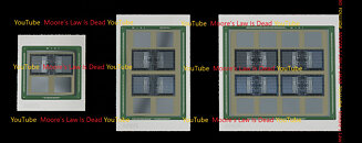
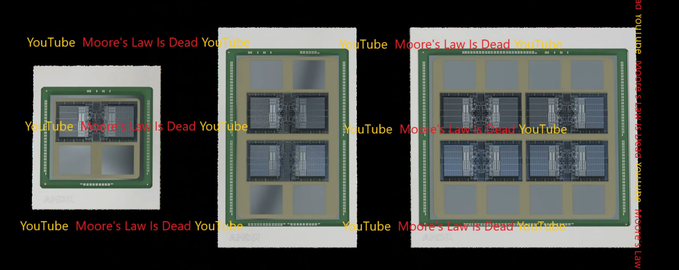
AMD's next-generation MI300 compute accelerator is expected to significantly scale up the logic density, according to a rumor by Moore's Law is Dead. Based on the CDNA3 compute architecture, the MI300 will be a monstrous large multi-chip module with as many as 8 logic dies (compute dies), each with its dedicated HBM3 stack. The compute dies (logic dies), will be 3D-stacked on top of I/O dies that pack the memory controllers, and the interconnect that performs the inter-die, and inter-package communication.

The report even goes on to mention that the compute die at the top level of the stack will be built on TSMC N5 (5 nm) silicon fabrication process, while the I/O die below will be TSMC N6 (6 nm). At this point it's not known if AMD will use the package to wire the logic stacks to the memory stacks, or whether it will take the pricier route of using a silicon interposer, but the report supports the interposer theory—that an all-encompassing interposer seats all eight compute dies, all four I/O dies (each with two compute dies), and the eight HBM3 stacks. An interposer is a silicon die that facilitates high density microscopic wiring between two dies on a package, which are otherwise not possible through large package substrate wiring.


View at TechPowerUp Main Site | Source
 
Just 600W ?
Nvidia wins the electric bill with 900W
 
Just 600W ?
Nvidia wins the electric bill with 900W

Yeah, next thing you know, the "people" in the Wccftech comments section will be attacking each other for having "peasant" circuit breakers and standard home wiring that can't handle it

"This peasant doesn't run 240V three phase! What a l4m3r"
 
Last edited:
Intel and AMD are the leaders in mcm gpu's.. nvidia will be left behind if they dnot do mcm.. monolith has its limits
 
Its not just MCM. 3D stacking of core logic is also important and so far AMD is the only one doing this.

Yeah, considering what AMD has accomplished so far, it makes you wonder what Lisa Su would be capable of if she had Intel's $15.19 Billion annual R&D budget or Nvidia's $5.27 billion instead of AMD's $2.84 Billion which, unlike Nvidia, has to be divided between x86 and GPU, and I think it's safe to assume that x86 gets substantially more than 50% of that budget considering the x86 has a much larger T.A.M, so it's impressive that AMD has been able to reach parity and in some cases surpass Nvidia in rasterization, and if current leaks are to be believed, might edge out Nvidia for performance in every category with RDNA3.

*Yes, Intel has many different areas its R&D budget must be divided amongst, but I'd be willing to bet the share it allocates to x86 and GPU are larger than AMD's respective allocations. Either way, when considering what AMD is able to achieve with its comparably smaller financial resources, it's seriously impressive.
 
Especially so when you consider they were nearly bankrupt 6 years back, though the last CEO also shares quite a bit of credit in this massive turnaround.
 
Its not just MCM. 3D stacking of core logic is also important and so far AMD is the only one doing this.

Intel is also doing that with Foveros and EMIB, though I believe neither is yet in mass production and only in very select products (but they actually own the technology instead of depending on tsmc for most of it)
 
Yeah, considering what AMD has accomplished so far, it makes you wonder what Lisa Su would be capable of if she had Intel's $15.19 Billion annual R&D budget or Nvidia's $5.27 billion instead of AMD's $2.84 Billion which, unlike Nvidia, has to be divided between x86 and GPU, and I think it's safe to assume that x86 gets substantially more than 50% of that budget considering the x86 has a much larger T.A.M, so it's impressive that AMD has been able to reach parity and in some cases surpass Nvidia in rasterization, and if current leaks are to be believed, might edge out Nvidia for performance in every category with RDNA3.

*Yes, Intel has many different areas its R&D budget must be divided amongst, but I'd be willing to bet the share it allocates to x86 and GPU are larger than AMD's respective allocations. Either way, when considering what AMD is able to achieve with its comparably smaller financial resources, it's seriously impressive.
For the budget AMD has, they are kicking both intel and nvidia in the balls over and over. Upward and Forward.
 
Yeah, next thing you know, the "people" in the Wccftech comments section will be attacking each other for having "peasant" circuit breakers and standard home wiring that can't handle it

"This peasant doesn't run 240V three phase! What a l4m3r"
Three phase is 400V...
71zBHoqVudL._SL1500_.jpg
 
For the budget AMD has, they are kicking both intel and nvidia in the balls over and over. Upward and Forward.
Especially that are no longer pretending to by your friendly neighborhood Pricederman.
 
So basically something resembling x8 RX 6400 XT's in a MCM design and I/O dies underneath that let them all communicate together!!? That or more of a die shrink on the RX 6400 XT bringing it up to parity with a RX 6500 XT plus any architectural changes if it's also RDNA3 as well!!? This is some amazing stuff. Funny how everything is resembling arcade boards and rom chips and stuff like the Atari STFM memory piggybacking scaled down to modern day manufacturing techniques and processes everything old is new again. The real magic is how they get it all to sync together from a engineering standpoint at reasonable latency what a achievement. It's sort of a LucidHydra concept all crunched together in a tidy package without all the latency complication concern troubles.
 
I had to look this up... In the US, you can have a 3-phase 240v? Its called a 3 Phase Open Delta (No clue what dafuq that means). Unless this website is completely wrong, I personally do not know. So this is a legit question. https://www.oempanels.com/240v-single-phase-and-240v-3-phase
In Europe, three phase is 400V and uses that connector. That said most people have never seen that connector, as it's not commonly used outside of construction sites and farms. At least where I come most people do have a 400V Volt socket, bit it's for cookers, so again, not something a lot of people have seen, unless they bought a new cooker.

Open Delta is usually without a neutral wire, the other kind of three phase, which again is common in Europe it's in a Y configuration with a neutral wire.
 
Last edited:
Open Delta is usually without a neutral wire, the other kind of three phase, which again is common in Europe it's in a Y configuration with a neutral wire.

Their (US and other split phase countries) and ours (Europe and other three phase countries) Open Delta is a bit different, they require a neutral on the Open delta and that neutral is not that "neutral" (the voltage to neutral is different on one of the phases). Our Delta configuration simply has no neutral (there's not even a place for it because the three phases are all the same, where the split system Delta has a neutral between the regular split phases).

Our Y config usually has a neutral connected in the center (between all phases) but it's not always necessary to included it for 3 phase loads.
I hate three phase, it's so damned complicated.
 
So basically something resembling x8 RX 6400 XT's in a MCM design and I/O dies underneath that let them all communicate together!!? That or more of a die shrink on the RX 6400 XT bringing it up to parity with a RX 6500 XT plus any architectural changes if it's also RDNA3 as well!!? This is some amazing stuff. Funny how everything is resembling arcade boards and rom chips and stuff like the Atari STFM memory piggybacking scaled down to modern day manufacturing techniques and processes everything old is new again. The real magic is how they get it all to sync together from a engineering standpoint at reasonable latency what a achievement. It's sort of a LucidHydra concept all crunched together in a tidy package without all the latency complication concern troubles.


Except instead of 12cu 768sp rdna3 chiplets they use CDNA3 chiplets of unknown config. But likely more cores in total than the current gen CDNA2 Mi250s, which used dual chiplet 104cu config, with 6656sp per cu.

So we aren't expecting 8k cores, current 250x already has more than that. We are expecting 2x-4x current cores.
 
Yeah I forgot AMD forked it's GPU designs still same idea just more compute focused. Wonder how quickly this will trickle down to consumers.
 
Back
Top