- Joined
- Aug 19, 2017
- Messages
- 2,543 (0.96/day)
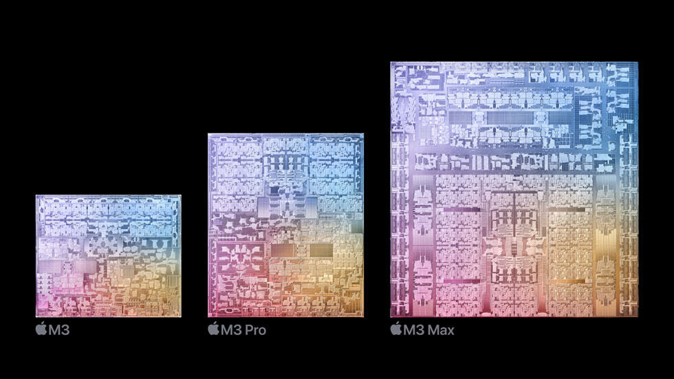
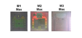
As we witness Apple's generational updates of the M series of chips, the highly anticipated SKU of the 3rd generation of Apple M series yet-to-be-announced top-of-the-line M3 Ultra chip is growing speculations from industry insiders. The latest round of reports suggests that the M3 Ultra might step away from its predecessor's design, potentially adopting a monolithic architecture without the UltraFusion interconnect technology. In the past, Apple has relied on a dual-chip design for its Ultra variants, using the UltraFusion interconnect to combine two M series Max chips. For example, the second generation M Ultra chip, M2 Ultra, boasts 134 billion transistors across two 510 mm² chips. However, die-shots of the M3 Max have sparked discussions about the absence of dedicated chip space for the UltraFusion interconnect.
While the absence of visible interconnect space on early die-shots is not conclusive evidence, as seen with the M1 Max not having visible UltraFusion interconnect and still being a part of M1 Ultra with UltraFusion, industry has led the speculation that the M3 Ultra may indeed feature a monolithic design. Considering that the M3 Max has 92 billion transistors and is estimated to have a die size between 600 and 700 mm², going Ultra with these chips may be pushing the manufacturing limit. Considering the maximum die size limit of 848 mm² for the TSMC N3B process used by Apple, there may not be sufficient space for a dual-chip M3 Ultra design. The potential shift to a monolithic design for the M3 Ultra raises questions about how Apple will scale the chip's performance without the UltraFusion interconnect. Competing solutions, such as NVIDIA's Blackwell GPU, use a high-bandwidth C2C interface to connect two 104 billion transistor chips, achieving a bandwidth of 10 TB/s. In comparison, the M2 Ultra's UltraFusion interconnect provided a bandwidth of 2.5 TB/s.
View at TechPowerUp Main Site | Source
While the absence of visible interconnect space on early die-shots is not conclusive evidence, as seen with the M1 Max not having visible UltraFusion interconnect and still being a part of M1 Ultra with UltraFusion, industry has led the speculation that the M3 Ultra may indeed feature a monolithic design. Considering that the M3 Max has 92 billion transistors and is estimated to have a die size between 600 and 700 mm², going Ultra with these chips may be pushing the manufacturing limit. Considering the maximum die size limit of 848 mm² for the TSMC N3B process used by Apple, there may not be sufficient space for a dual-chip M3 Ultra design. The potential shift to a monolithic design for the M3 Ultra raises questions about how Apple will scale the chip's performance without the UltraFusion interconnect. Competing solutions, such as NVIDIA's Blackwell GPU, use a high-bandwidth C2C interface to connect two 104 billion transistor chips, achieving a bandwidth of 10 TB/s. In comparison, the M2 Ultra's UltraFusion interconnect provided a bandwidth of 2.5 TB/s.


View at TechPowerUp Main Site | Source


