Raevenlord
News Editor
- Joined
- Aug 12, 2016
- Messages
- 3,755 (1.18/day)
- Location
- Portugal
| System Name | The Ryzening |
|---|---|
| Processor | AMD Ryzen 9 5900X |
| Motherboard | MSI X570 MAG TOMAHAWK |
| Cooling | Lian Li Galahad 360mm AIO |
| Memory | 32 GB G.Skill Trident Z F4-3733 (4x 8 GB) |
| Video Card(s) | Gigabyte RTX 3070 Ti |
| Storage | Boot: Transcend MTE220S 2TB, Kintson A2000 1TB, Seagate Firewolf Pro 14 TB |
| Display(s) | Acer Nitro VG270UP (1440p 144 Hz IPS) |
| Case | Lian Li O11DX Dynamic White |
| Audio Device(s) | iFi Audio Zen DAC |
| Power Supply | Seasonic Focus+ 750 W |
| Mouse | Cooler Master Masterkeys Lite L |
| Keyboard | Cooler Master Masterkeys Lite L |
| Software | Windows 10 x64 |
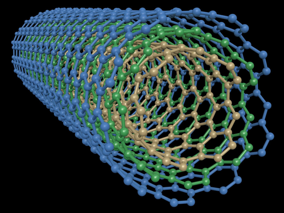
Graphene has been hailed for some time now as the next natural successor to silicon, today's most used medium for semiconductor technology. However, even before such more exotic solutions to current semiconductor technology are employed (and we are still way off that future, at least when it comes to mass production), engineers and researchers seem to be increasing their focus in one specific part of computing: internal communication between components.
Typically, communication between a computer's Central Processing Unit (CPU) and a system's memory (usually DRAM) have occurred through a bus, which is essentially a communication highway between data stored in the DRAM, and the data that the CPU needs to process/has just finished processing. The fastest CPU and RAM is still only as fast as the bus, and recent workloads have been increasing the amount of data to be processed (and thus transferred) by orders of magnitude. As such, engineers have been trying to figure out ways of increasing communication speed between the CPU and the memory subsystem, as it is looking increasingly likely that the next bottlenecks in HPC will come not through lack of CPU speed or memory throughput, but from a bottleneck in communication between those two.
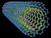
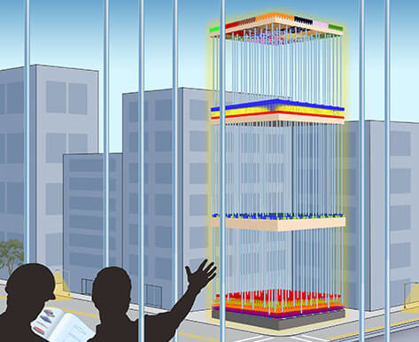
The MIT and Stanford researchers' solution? Do away with a bus entirely, by entwining the CPU and memory together so closely that there is no need for performance bottle-necking buses. According to the lead author in the research paper, Max Shulaker, "The RRAM and carbon nanotubes are built vertically over one another, making a new, dense 3-D computer architecture with interleaving layers of logic and memory. By inserting ultradense wires between these layers, this 3-D architecture promises to address the communication bottleneck." As a proof of concept (let's call it PoC for the Mass Effect: Andromeda fans out there), the team has produced a small-scale carbon nanotube (CNT) computer, and get this: it was actually capable of running programs, a basic multitasking operating system, and performing MIPS instructions. The pairing with RRAM (Resistive Random Access Memory) is a feat unto itself, as H.-S. Philip Wong, a co-author of the research, says that "RRAM can be denser, faster, and more energy-efficient compared to DRAM." In-between the logic and memory layers are "ultradense" wires that provide communication, which is "more than an order of magnitude" faster and more energy efficient than silicon.

Granted, the new system likely won't break speed records soon - it ran at 1 kHz. However, researchers behind the paper claim that achieving higher speeds is a more trivial task compared to the actual development of this unit in particular. As they put it, the speed limit "(...) is not due to the limitations of the CNT technology or our design methodology, but instead is caused by capacitive loading introduced by the measurement setup, the 1-mm minimum lithographic feature size possible in our academic fabrication facility, and CNT density and contact resistance." Compare the university's 1-mm minimum litographic feature size they can possibly achieve with their tools with those currently employed by state-of-the-art foundries by the likes of Intel and Samsung, and you're likely to even more respect the scientist's achievement. Even so, "the researchers integrated over 1 million RRAM cells and 2 million carbon nanotube field-effect transistors, making the most complex nanoelectronic system ever made with emerging nanotechnologies."

One of the key benefits of fabricating the new computer chips from graphene stems from the much lower temperatures involved in fabrication - and is what makes such a marriage between a CPU and its memory all but impossible through silicon. Silicon chip creation requires temperatures up to 1,000 degrees Celsius, so it's difficult to make multi-layers and 3D structures without damaging prior layers. However, "carbon nanotube circuits and RRAM memory can be fabricated at much lower temperatures, below 200°C", says Shulaker, which enables the stacking and interlinking of memory and CPU through fine wires.
View at TechPowerUp Main Site
Typically, communication between a computer's Central Processing Unit (CPU) and a system's memory (usually DRAM) have occurred through a bus, which is essentially a communication highway between data stored in the DRAM, and the data that the CPU needs to process/has just finished processing. The fastest CPU and RAM is still only as fast as the bus, and recent workloads have been increasing the amount of data to be processed (and thus transferred) by orders of magnitude. As such, engineers have been trying to figure out ways of increasing communication speed between the CPU and the memory subsystem, as it is looking increasingly likely that the next bottlenecks in HPC will come not through lack of CPU speed or memory throughput, but from a bottleneck in communication between those two.
The MIT and Stanford researchers' solution? Do away with a bus entirely, by entwining the CPU and memory together so closely that there is no need for performance bottle-necking buses. According to the lead author in the research paper, Max Shulaker, "The RRAM and carbon nanotubes are built vertically over one another, making a new, dense 3-D computer architecture with interleaving layers of logic and memory. By inserting ultradense wires between these layers, this 3-D architecture promises to address the communication bottleneck." As a proof of concept (let's call it PoC for the Mass Effect: Andromeda fans out there), the team has produced a small-scale carbon nanotube (CNT) computer, and get this: it was actually capable of running programs, a basic multitasking operating system, and performing MIPS instructions. The pairing with RRAM (Resistive Random Access Memory) is a feat unto itself, as H.-S. Philip Wong, a co-author of the research, says that "RRAM can be denser, faster, and more energy-efficient compared to DRAM." In-between the logic and memory layers are "ultradense" wires that provide communication, which is "more than an order of magnitude" faster and more energy efficient than silicon.
Granted, the new system likely won't break speed records soon - it ran at 1 kHz. However, researchers behind the paper claim that achieving higher speeds is a more trivial task compared to the actual development of this unit in particular. As they put it, the speed limit "(...) is not due to the limitations of the CNT technology or our design methodology, but instead is caused by capacitive loading introduced by the measurement setup, the 1-mm minimum lithographic feature size possible in our academic fabrication facility, and CNT density and contact resistance." Compare the university's 1-mm minimum litographic feature size they can possibly achieve with their tools with those currently employed by state-of-the-art foundries by the likes of Intel and Samsung, and you're likely to even more respect the scientist's achievement. Even so, "the researchers integrated over 1 million RRAM cells and 2 million carbon nanotube field-effect transistors, making the most complex nanoelectronic system ever made with emerging nanotechnologies."

One of the key benefits of fabricating the new computer chips from graphene stems from the much lower temperatures involved in fabrication - and is what makes such a marriage between a CPU and its memory all but impossible through silicon. Silicon chip creation requires temperatures up to 1,000 degrees Celsius, so it's difficult to make multi-layers and 3D structures without damaging prior layers. However, "carbon nanotube circuits and RRAM memory can be fabricated at much lower temperatures, below 200°C", says Shulaker, which enables the stacking and interlinking of memory and CPU through fine wires.
View at TechPowerUp Main Site
Last edited by a moderator:


