- Joined
- Oct 9, 2007
- Messages
- 47,878 (7.38/day)
- Location
- Dublin, Ireland
| System Name | RBMK-1000 |
|---|---|
| Processor | AMD Ryzen 7 5700G |
| Motherboard | Gigabyte B550 AORUS Elite V2 |
| Cooling | DeepCool Gammax L240 V2 |
| Memory | 2x 16GB DDR4-3200 |
| Video Card(s) | Galax RTX 4070 Ti EX |
| Storage | Samsung 990 1TB |
| Display(s) | BenQ 1440p 60 Hz 27-inch |
| Case | Corsair Carbide 100R |
| Audio Device(s) | ASUS SupremeFX S1220A |
| Power Supply | Cooler Master MWE Gold 650W |
| Mouse | ASUS ROG Strix Impact |
| Keyboard | Gamdias Hermes E2 |
| Software | Windows 11 Pro |
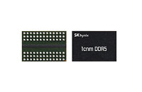
SK hynix announced today that it has developed the industry's first 16 Gb DDR5 built using its 1c node, the sixth generation of the 10 nm process. The success marks the beginning of the extreme scaling to the level closer to 10 nm in the memory process technology. The degree of difficulty to advance the shrinking process of the 10 nm-range DRAM technology has grown over generations, but SK hynix has become the first in the industry to overcome the technological limitations by raising the level of completion in design, thanks to its industry-leading technology of the 1b, the fifth generation of the 10 nm process.
SK hynix said it will be ready for mass production of the 1c DDR5 within the year to start volume shipment next year. In order to reduce potential errors stemming from the procedure of advancing the process and transfer the advantage of the 1b, which is widely applauded for its best performing DRAM, in the most efficient way, the company extended the platform of the 1b DRAM for development of 1c. The new product comes with an improvement in cost competitiveness, compared with the previous generation, by adopting a new material in certain process of the extreme ultraviolet, or EUV, while optimizing the EUV application process of total. SK hynix also enhanced productivity by more than 30% through technological innovation in design.

The operating speed of the 1c DDR5, expected to be adopted for high-performance data centers, is improved by 11% from the previous generation, to 8 Gbps. With power efficiency also improved by more than 9%, SK hynix expects adoption of 1c DRAM to help data centers reduce the electricity cost by as much as 30% at a time when advancement of AI era is leading to an increase in power consumption.
"We are committed to providing differentiated values to customers by applying the 1c technology equipped with the best performance and cost competitiveness to our major next-generation products including HBM, LPDDR6, and GDDR7," said Head of DRAM Development Kim Jonghwan. "We will continue to work towards maintaining the leadership in the DRAM space and position as the most-trusted AI memory solution provider."
View at TechPowerUp Main Site
SK hynix said it will be ready for mass production of the 1c DDR5 within the year to start volume shipment next year. In order to reduce potential errors stemming from the procedure of advancing the process and transfer the advantage of the 1b, which is widely applauded for its best performing DRAM, in the most efficient way, the company extended the platform of the 1b DRAM for development of 1c. The new product comes with an improvement in cost competitiveness, compared with the previous generation, by adopting a new material in certain process of the extreme ultraviolet, or EUV, while optimizing the EUV application process of total. SK hynix also enhanced productivity by more than 30% through technological innovation in design.

The operating speed of the 1c DDR5, expected to be adopted for high-performance data centers, is improved by 11% from the previous generation, to 8 Gbps. With power efficiency also improved by more than 9%, SK hynix expects adoption of 1c DRAM to help data centers reduce the electricity cost by as much as 30% at a time when advancement of AI era is leading to an increase in power consumption.
"We are committed to providing differentiated values to customers by applying the 1c technology equipped with the best performance and cost competitiveness to our major next-generation products including HBM, LPDDR6, and GDDR7," said Head of DRAM Development Kim Jonghwan. "We will continue to work towards maintaining the leadership in the DRAM space and position as the most-trusted AI memory solution provider."
View at TechPowerUp Main Site


