T0@st
News Editor
- Joined
- Mar 7, 2023
- Messages
- 3,283 (4.00/day)
- Location
- South East, UK
| System Name | The TPU Typewriter |
|---|---|
| Processor | AMD Ryzen 5 5600 (non-X) |
| Motherboard | GIGABYTE B550M DS3H Micro ATX |
| Cooling | DeepCool AS500 |
| Memory | Kingston Fury Renegade RGB 32 GB (2 x 16 GB) DDR4-3600 CL16 |
| Video Card(s) | PowerColor Radeon RX 7800 XT 16 GB Hellhound OC |
| Storage | Samsung 980 Pro 1 TB M.2-2280 PCIe 4.0 X4 NVME SSD |
| Display(s) | Lenovo Legion Y27q-20 27" QHD IPS monitor |
| Case | GameMax Spark M-ATX (re-badged Jonsbo D30) |
| Audio Device(s) | FiiO K7 Desktop DAC/Amp + Philips Fidelio X3 headphones, or ARTTI T10 Planar IEMs |
| Power Supply | ADATA XPG CORE Reactor 650 W 80+ Gold ATX |
| Mouse | Roccat Kone Pro Air |
| Keyboard | Cooler Master MasterKeys Pro L |
| Software | Windows 10 64-bit Home Edition |
Tokyo Electron announced that its development team at Tokyo Electron Miyagi—the development and manufacturing site for its plasma etch systems—has developed an innovative etch technology capable of producing memory channel holes in advanced 3D NAND devices with a stack of over 400 layers. The new process developed by the team has brought dielectric etch application to the cryogenic temperature range for the first time, producing a system with exceptionally high etch rates.
The innovative technology not only enables a 10-µm-deep etch with a high aspect ratio in just 33 minutes, but also can reduce the global warming potential by 84% compared with previous technologies. The geometry of the etched structure is quite well-defined as shown in the figure 1. Potential innovations enabled by this technology will spur creation of 3D NAND flash memory with even larger capacity.


Figure 1 shows a cross section SEM image of memory channel hole pattern after etching, and FIB cut image at the hole bottom. Figure 2 is an example of TEL's 3D NAND Flash.
TEL's team that developed this technology will present a report on its research results at the 2023 Symposium on VLSI Technology and Circuits, one of the most prestigious international conferences on semiconductor research, to be held from June 11 to June 16 in Kyoto. Please look forward to our technology presentation that contributes to semiconductor technology innovation and global environment protection.
Continuing to pursue the motto of Best Products and Best Technical Service, TEL will contribute to technological innovation in semiconductors. As this year marks the 60th anniversary of our founding—which we consider to be a new transformative point for us—we will take on new challenges and continue to evolve, contributing to the development of a dream-inspiring society.
View at TechPowerUp Main Site | Source
The innovative technology not only enables a 10-µm-deep etch with a high aspect ratio in just 33 minutes, but also can reduce the global warming potential by 84% compared with previous technologies. The geometry of the etched structure is quite well-defined as shown in the figure 1. Potential innovations enabled by this technology will spur creation of 3D NAND flash memory with even larger capacity.

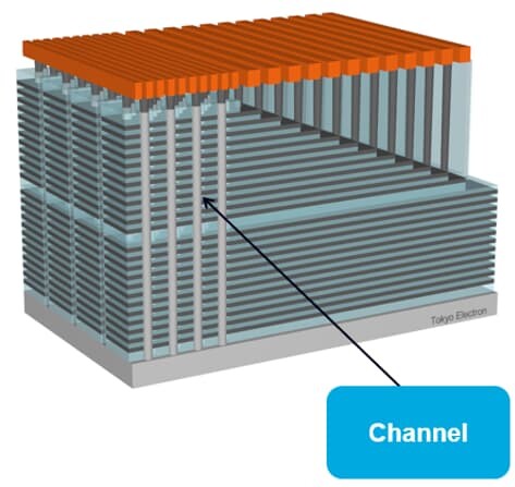
Figure 1 shows a cross section SEM image of memory channel hole pattern after etching, and FIB cut image at the hole bottom. Figure 2 is an example of TEL's 3D NAND Flash.
TEL's team that developed this technology will present a report on its research results at the 2023 Symposium on VLSI Technology and Circuits, one of the most prestigious international conferences on semiconductor research, to be held from June 11 to June 16 in Kyoto. Please look forward to our technology presentation that contributes to semiconductor technology innovation and global environment protection.
Continuing to pursue the motto of Best Products and Best Technical Service, TEL will contribute to technological innovation in semiconductors. As this year marks the 60th anniversary of our founding—which we consider to be a new transformative point for us—we will take on new challenges and continue to evolve, contributing to the development of a dream-inspiring society.
View at TechPowerUp Main Site | Source


