• Welcome to TechPowerUp Forums, Guest! Please check out our forum guidelines for info related to our community.
  • The forums have been upgraded with support for dark mode. By default it will follow the setting on your system/browser. You may override it by scrolling to the end of the page and clicking the gears icon.

TSMC N3 Nodes Show SRAM Scaling is Hitting the Wall

AleksandarK

News Editor
Staff member
Joined
Aug 19, 2017
Messages
3,149 (1.10/day)
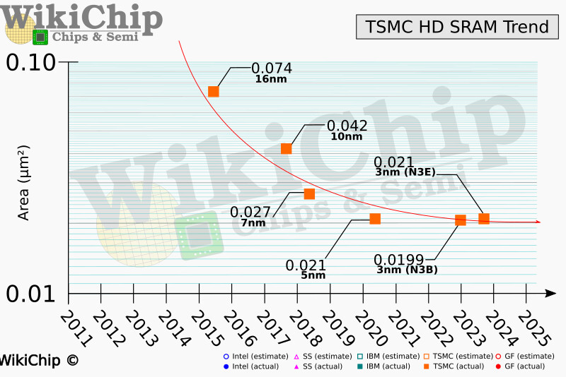
When TSMC introduced its N3 lineup of nodes, the company only talked about the logic scaling of the two new semiconductor manufacturing steps. However, it turns out that there was a reason for it, as WikiChip confirms that the SRAM bit cells of N3 nodes are almost identical to the SRAM bit cells of N5 nodes. At TSMC 2023 Technology Symposium, TSMC presented additional details about its N3 node lineup, including logic and SRAM density. For starters, the N3 node is TSMC's "3 nm" node family that has two products: a Base N3 node (N3B) and an Enhanced N3 node (N3E). The base N3B uses a new (for TSMC) self-aligned contact (SAC) scheme that Intel introduced back in 2011 with a 22 nm node, which improves the node's yield.

Regardless of N3's logic density improvements compared to the "last-generation" N5, the SRAM density is almost identical. Initially, TSMC claimed N3B SRAM density was 1.2x over the N5 process. However, recent information shows that the actual SRAM density is merely a 5% difference. With SRAM taking a large portion of the transistor and area budget of a processor, N3B's soaring manufacturing costs are harder to justify when there is almost no area improvement. For some time, SRAM scaling wasn't following logic scaling; however, the two have now completely decoupled.


View at TechPowerUp Main Site | Source
 
When you take the time to look at the graph and realize its logarithmic on the area, it has been flatlined since 5nm, and if you include 7nm, it's still a pretty flat line.
 
How long until the SRAM is on a separate chip entirely (think X3D style) and the logic chip is only cores and interconnect?
 
Backside power delivery, or PowerVia in Intel parlance, should help with SRAM scaling. Nanosheet transistors will also help, but these are all slated for either Intel's 20A node or TSMC's N2P node. These aren't expected to be available until 2024 and 2026 respectively.

How long until the SRAM is on a separate chip entirely (think X3D style) and the logic chip is only cores and interconnect?
That will increase latency of SRAM as off-chip communication is costly in both latency and power. It could only be done with large, last level caches like AMD's LLC for RDNA3. Smaller caches like L1 and L2 will remain on-chip.
 
It's a miracle that some SRAM scaling still fits between 7nm and 3nm. ASML's 3000 series(3400&3600) lithography scanners are both fully identical wavelengths.
Screenshot_2023-05-29-21-01-17-40_40deb401b9ffe8e1df2f1cc5ba480b12.jpg
 
It's a miracle that some SRAM scaling still fits between 7nm and 3nm. ASML's 3000 series(3400&3600) lithography scanners are both fully identical wavelengths.
It's not a miracle. The light source is a necessary part of the process, but it doesn't govern the minimum size of the current processes which are all greater than 13.5 nm. Besides, N7 doesn't use EUV. Instead, it uses light with a wavelength of 193 nm.
 
It's a miracle that some SRAM scaling still fits between 7nm and 3nm. ASML's 3000 series(3400&3600) lithography scanners are both fully identical wavelengths.
View attachment 298202
Any chance of any new scanners having shorter wavelengths then? If we can't go further than that we'll be stuck with the chips only getting tiny improvements.
 
How long until the SRAM is on a separate chip entirely (think X3D style) and the logic chip is only cores and interconnect?
You answered your own question x3D already brought that.

First off die would be L3, they're not getting the L1/2 cache's off die, the optic chips or another massive in memory compute evolution is necessary to change that I think.
 
there is no problem with small size of caches, but problem with unoptimized software.
For well optimized software, few magabytes of cache is sufficient
In the real world, the working set of most programs isn't defined by their code. Perhaps you have heard of servers that usually have hundreds of GB of RAM. Do you think they would do fine with CPUs with less than 10 MB of last level cache.
Yes, N7 doesn't use EUV, but there is much more than one "7"nm variants.
True, but the most popular variant is the one that forgoes EUV.
 
Backside power delivery, or PowerVia in Intel parlance, should help with SRAM scaling. Nanosheet transistors will also help, but these are all slated for either Intel's 20A node or TSMC's N2P node. These aren't expected to be available until 2024 and 2026 respectively.


That will increase latency of SRAM as off-chip communication is costly in both latency and power. It could only be done with large, last level caches like AMD's LLC for RDNA3. Smaller caches like L1 and L2 will remain on-chip.
With proper die stacking there is no large latency penalty, heck it might even be lower due to lower distance in z direction compared to x-y.

What is a problem though is heat dissipation, which is why it currently is limited to the LLC of Zen3/4, because of its lower power density compared to the core area.
Still the X3D chips run much hotter due to the structural silicon pieces, but would be even hotter if it was covered with active silicon.
I was thinking of non stacked chips, but your're right; die stacking solves the downsides of off-chip cache, but in its current form, it brings new issues too.
 
Any chance of any new scanners having shorter wavelengths then? If we can't go further than that we'll be stuck with the chips only getting tiny improvements.
Yes 5000 series. Very first 5000 are delivered to Intel. First 5200 will be delivered in 2024.
 
Any chance of any new scanners having shorter wavelengths then? If we can't go further than that we'll be stuck with the chips only getting tiny improvements.
With all of lithography the process of converting to a "shorter wavelength" means either an optical improvement (lenses/mirrors) or a new light source. At this point, there's not many good candidates for a new light source sub 13.5nm. Like someone else said in the thread, the ASML EXE platform is the next step on the optics side of things to reduce the wavelength. The platform is also called High NA (Numerical Aperture), and essentially allow for wavelength reductions down to around 8nm. The core design behind how the light source is generated, however, remains the same as the current EUV tools.

For more information on how these minimium resolutions are calculated, you can look into the Rayleigh Criterion, which is basically what governs all of this in terms of minimum critical dimension
 
Can't the mosfet's be stacked so the sram cell is flipped 90°?
That would describe the CFET (complementary FET), which is a stack of two transistors. Yes, just two. And I'm not sure anyone has produced even an experimental working chip with those.
 
Any chance of any new scanners having shorter wavelengths then? If we can't go further than that we'll be stuck with the chips only getting tiny improvements.
From what I heard that 13.5nm is the optimal wavelength to etch on current materials as anything smaller tends to go through the material vs reflect/etch


So it will probably take a massive leap in materials technolgy again to get the next "leap" vs just optimising 13.5nm utilisation.
 
Smaller caches like L1 and L2 will remain on-chip.
AMD said the stacked L3 chip adds four clock cycles to access latency. Assuming the same were true for L2, it might actually be beneficial if a Zen core could have, for example, 1 MB plus stacked 2 MB of L2 compared to just 1 MB of faster L2.
 
FbYOsFqVUAEVcQZ.jpg
WuHAyr6QC7Ch2JCm.jpg


L1 and L2 are nothing compared to the vast expanse of L3.

What seems likely is a "blank area" where the L3 sits currently, with interconnects on-chip but no actual transistors. Then the L3, made on a larger node, is laid in the same area but is considerably higher capacity.
 
L1 and L2 are nothing compared to the vast expanse of L3.
What do you mean, nothing? 1 MB of L2 is about one third the size of a slice of L3 (= 4 MB next to each core).
 
What do you mean, nothing? 1 MB of L2 is about one third the size of a slice of L3 (= 4 MB next to each core).
You have 4X the L3 as L2, and that is on Zen 4. I understand that L3 sizes are going to increase again pretty soon.
 
Back
Top