Report an Error
Samsung 850 EVO 500 GB (Samsung V2)
500 GB
Capacity
Samsung MGX
Controller
TLC
Flash
SATA 6 Gbps
Interface
2.5"
Form Factor
Multiple hardware versions found.
Performance could vary due to unannounced flash/controller changes.


Back

AnandTech
PCB Front

AnandTech
DRAM
AnandTech
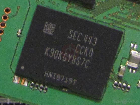
Flash

Controller

NAND Die
The Samsung 850 EVO was a solid-state drive in the 2.5" form factor, launched on December 8th, 2014, that is no longer in production. It was available in capacities ranging from 120 GB to 2 TB. This page reports specifications for the 500 GB variant. With the rest of the system, the Samsung 850 EVO interfaces using a SATA 6 Gbps connection. The SSD controller is the MGX (S4LN062X01) from Samsung, a DRAM cache chip is available. Samsung has installed 32-layer TLC NAND flash on the 850 EVO, the flash chips are made by Samsung. Please note that this SSD is sold in multiple variants with different NAND flash or controller, which could affect performance, the "Notes" section at the end of this page has more info. To improve write speeds, a pseudo-SLC cache is used, so bursts of incoming writes are handled more quickly. The cache is sized at 6 GB, once it is full, writes complete at 500 MB/s. The 850 EVO is rated for sequential read speeds of up to 540 MB/s and 520 MB/s write; random IO reaches 90K IOPS for read and 98K for writes.
At its launch, the SSD was priced at 270 USD. The warranty length is set to five years, which is an excellent warranty period. Samsung guarantees an endurance rating of 150 TBW, a relatively low value compared to other SSDs.
At its launch, the SSD was priced at 270 USD. The warranty length is set to five years, which is an excellent warranty period. Samsung guarantees an endurance rating of 150 TBW, a relatively low value compared to other SSDs.
Solid-State-Drive
| Capacity: | 500 GB |
|---|---|
| Variants: | 120 GB 250 GB 500 GB 1 TB 2 TB |
| Hardware Versions: | |
| Overprovisioning: | 46.3 GB / 10.0 % |
| Production: | End-of-life |
| Released: | Dec 8th, 2014 |
| Price at Launch: | 270 USD |
| Part Number: | MZ-75E500 |
| Market: | Consumer |
Physical
| Form Factor: | 2.5" |
|---|---|
| Interface: | SATA 6 Gbps |
| Protocol: | AHCI |
| Power Draw: |
0.05 W (Idle) 3.7 W (Avg) 4.4 W (Max) |
Controller
| Manufacturer: | Samsung |
|---|---|
| Name: | MGX (S4LN062X01) |
| Architecture: | ARM 32-bit Cortex R4 |
| Core Count: | Dual-Core |
| Frequency: | 550 MHz |
| Foundry: | Samsung |
| Process: | 32 nm |
| Flash Channels: | 8 |
| Chip Enables: | 8 |
NAND Flash
| Manufacturer: | Samsung |
|---|---|
| Name: | V-NAND V2 |
| Part Number: | K9OKGY8S7C-CCK0 |
| Type: | TLC |
| Technology: | 32-layer |
| Speed: | 533 MT/s .. 1000 MT/s |
| Capacity: | 4 chips @ 1 Tbit |
| Topology: | Charge Trap |
| Process: | 40 nm |
| Die Size: | 69 mm² (1.9 Gbit/mm²) |
| Dies per Chip: | 8 dies @ 128 Gbit |
| Planes per Die: | 1 |
| Decks per Die: | 1 |
| Word Lines: |
39 per NAND String
82.1% Vertical Efficiency |
| Read Time (tR): | 45 µs |
| Program Time (tProg): | 700 µs |
| Block Erase Time (tBERS): | 3500 ms |
| Die Write Speed: | 50 MB/s |
| Endurance: (up to) |
7000 P/E Cycles
(20500 in SLC Mode) |
| Page Size: | 16 KB |
| Block Size: | 384 Pages |
| Plane Size: | 2732 Blocks |
DRAM Cache
| Type: | LPDDR2-1066 |
|---|---|
| Name: | SAMSUNG K4E4E164EE-SGCE |
| Capacity: |
512 MB
(1x 512 MB) |
| Organization: | 4Gx16 |
Performance
| Sequential Read: | 540 MB/s |
|---|---|
| Sequential Write: | 520 MB/s |
| Random Read: | 90,000 IOPS |
| Random Write: | 98,000 IOPS |
| Endurance: | 150 TBW |
| Warranty: | 5 Years |
| MTBF: | 1.5 Million Hours |
| Drive Writes Per Day (DWPD): | 0.2 |
| SLC Write Cache: |
approx. 6 GB
(static only) |
| Speed when Cache Exhausted: | approx. 500 MB/s |
Features
| TRIM: | Yes |
|---|---|
| SMART: | Yes |
| Power Loss Protection: | No |
| Encryption: |
|
| RGB Lighting: | No |
| PS5 Compatible: | No |
Reviews
Notes
Drive:Rev 2: SAMSUNG V3 V-NAND 48-Layers Controller:Could be 4 or 8 Channels NAND Die:tPROG with overhead: 700 µs (Avg 45.7 MB/s per die) |
Jun 1st, 2024 16:31 EDT
change timezone
Latest GPU Drivers
New Forum Posts
- Really interesting new Cycle HUB design. (1)
- Core counting (59)
- Is 8gb enough for games in 1440p in 2024 ? (99)
- clear partitions and reset nvme firecudaa 520 (7)
- What's your latest tech purchase? (20713)
- PC Build for customer arrived damage (0)
- random shut down-PSU issue? (27)
- What is unverified VBIOS? (8)
- seeking advice about a new build (2)
- How do you get games for PC? (9)
Popular Reviews
- ID-Cooling FX360 PRO Review - Shots Fired @ Arctic
- SilverStone KL07E Review
- NuPhy Air96 V2 Low Profile Wireless Mechanical Keyboard Review
- Senua’s Saga: Hellblade II: DLSS vs. FSR vs. XeSS Comparison Review
- Upcoming Hardware Launches 2024 (Updated May 2024)
- Montech Titan Gold 1000 W Review
- Elysian Acoustic Labs Pilgrim In-Ear Monitors Review
- Waizowl OGM Cloud Review
- Ghost of Tsushima Performance Benchmark Review - 35 GPUs Tested
- Senua's Saga: Hellblade II Performance Benchmark Review
Controversial News Posts
- AMD to Redesign Ray Tracing Hardware on RDNA 4 (227)
- NVIDIA to Only Launch the Flagship GeForce RTX 5090 in 2024, Rest of the Series in 2025 (154)
- AMD Hits Highest-Ever x86 CPU Market Share in Q1 2024 Across Desktop and Server (140)
- AMD RDNA 5 a "Clean Sheet" Graphics Architecture, RDNA 4 Merely Corrects a Bug Over RDNA 3 (139)
- NVIDIA RTX 5090 "Blackwell" Founders Edition to Implement the "RTX 4090 Ti" Cinderblock Design (116)
- Core Configurations of Intel Core Ultra 200 "Arrow Lake-S" Desktop Processors Surface (101)
- Biden Administration to Revive Trump-Era Tariffs on China-made GPUs and Motherboards (95)
- AMD Ryzen 9000 Zen 5 Single Thread Performance at 5.80 GHz Found 19% Over Zen 4 (86)