- Joined
- Oct 9, 2007
- Messages
- 47,901 (7.37/day)
- Location
- Dublin, Ireland
| System Name | RBMK-1000 |
|---|---|
| Processor | AMD Ryzen 7 5700G |
| Motherboard | Gigabyte B550 AORUS Elite V2 |
| Cooling | DeepCool Gammax L240 V2 |
| Memory | 2x 16GB DDR4-3200 |
| Video Card(s) | Galax RTX 4070 Ti EX |
| Storage | Samsung 990 1TB |
| Display(s) | BenQ 1440p 60 Hz 27-inch |
| Case | Corsair Carbide 100R |
| Audio Device(s) | ASUS SupremeFX S1220A |
| Power Supply | Cooler Master MWE Gold 650W |
| Mouse | ASUS ROG Strix Impact |
| Keyboard | Gamdias Hermes E2 |
| Software | Windows 11 Pro |
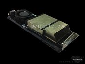
Here is a brief compilation of all the new images of the upcoming NVIDIA GeForce Kepler high-performance product, which our forum members posted through the day. The pictures reinforce the 3QTR picture that surfaced this Thursday, and full-length picture of the PCB that surfaced earlier this month. The first picture below, reveals what is essentially the card that was pictured yesterday, with its cooler shroud taken out. You will find a conventional air-channel cooler design. A lateral-flow fan, which looks similar to the one used in GeForce GTX 580/570), directs air through a dense aluminum channel array, which draws heat from key components such as the GPU, memory, and VRM, using a vapor-chamber plate (again, similar to the one used on high-end GeForce GTX 500 series). Towards the rear portion, you'll spot the piggy-backed 6+6-pin PCIe power connector cluster. You will also find the black rugged metal base-plate flowing along the full length of the PCB, structurally reinforcing it, and performing some cooling functions.
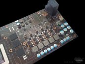
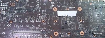
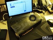
Moving on, the second picture reveals the same VRM area we saw earlier, on the green-colored PCB engineering sample, with its five NVVDD phases. The third picture is the first, of the reverse side of the PCB. Revealing most of the solder points, and electrical circuitry. The driver ICs of each of the NVVDD phases can be seen here. These two pictures confirm that the retail version of the GK104 product will feature a black PCB (the brown tinge is natural, due to the dense network of traces and ground layers, made of copper). The fourth picture reveals what looks like NVIDIA's Media Kit. Reputed reviewers get a NVIDIA-branded "media kit", which contains the graphics card sample to review, and other relevant documentation in printed form, along with a driver CD, and other accessories. These cards are not branded by any AIC partner, and are 100% compliant to NVIDIA's reference design and clock speeds.
Many Thanks to our community members JaredPace and CrapDaddy.
View at TechPowerUp Main Site
Moving on, the second picture reveals the same VRM area we saw earlier, on the green-colored PCB engineering sample, with its five NVVDD phases. The third picture is the first, of the reverse side of the PCB. Revealing most of the solder points, and electrical circuitry. The driver ICs of each of the NVVDD phases can be seen here. These two pictures confirm that the retail version of the GK104 product will feature a black PCB (the brown tinge is natural, due to the dense network of traces and ground layers, made of copper). The fourth picture reveals what looks like NVIDIA's Media Kit. Reputed reviewers get a NVIDIA-branded "media kit", which contains the graphics card sample to review, and other relevant documentation in printed form, along with a driver CD, and other accessories. These cards are not branded by any AIC partner, and are 100% compliant to NVIDIA's reference design and clock speeds.


Many Thanks to our community members JaredPace and CrapDaddy.
View at TechPowerUp Main Site


 JaredPace and CrapDaddy, THANKS!