- Joined
- Oct 9, 2007
- Messages
- 47,849 (7.39/day)
- Location
- Dublin, Ireland
| System Name | RBMK-1000 |
|---|---|
| Processor | AMD Ryzen 7 5700G |
| Motherboard | Gigabyte B550 AORUS Elite V2 |
| Cooling | DeepCool Gammax L240 V2 |
| Memory | 2x 16GB DDR4-3200 |
| Video Card(s) | Galax RTX 4070 Ti EX |
| Storage | Samsung 990 1TB |
| Display(s) | BenQ 1440p 60 Hz 27-inch |
| Case | Corsair Carbide 100R |
| Audio Device(s) | ASUS SupremeFX S1220A |
| Power Supply | Cooler Master MWE Gold 650W |
| Mouse | ASUS ROG Strix Impact |
| Keyboard | Gamdias Hermes E2 |
| Software | Windows 11 Pro |
Some of the first die-shots and annotations of the Intel Core Ultra 200V "Lunar Lake" processor surfaced on the web, thanks to die-shots by GeenWens and Kurnalsalts on Twitter. Be sure to check out our Lunar Lake Technical Deep-dive article to learn the basics of how Lunar Lake is different from "Meteor Lake." Both are disaggregated chiplet-based processors, but Lunar Lake remodels things a bit. All the logic engines of the processor—the CPU, the iGPU, and the NPU, are located in a centralized Compute tile that's built on the TSMC 3 nm process, while all the I/O controllers are spun out to the Platform Controller tile built on TSMC 6 nm, which sit on a Foveros base tile that acts as an interposer, facilitating high-density microscopic connections between the two tiles. The base tile sits on the fiberglass substrate, which also has stacked LPDDR5X memory for either 16 GB or 32 GB of on-package system memory.
The Kurnalsalts annotation provides a good lay of the land for the Compute tile. The most striking aspect of it is the CPU. "Lunar Lake" comes with a 4P+4E core hybrid CPU, but the two kinds of cores do not share a last-level cache or sit in a ringbus, unlike in case of the Compute tile of "Meteor Lake." The four "Lion Cove" P-cores each come with 2.5 MB of dedicated L2 caches, and share a 12 MB L3 cache. The four "Skymont" E-cores are not part of the ringbus connecting the four P-cores, rather they are physically separated, much like the low-power island E-cores on "Meteor Lake." The E-core cluster shares a 4 MB L2 cache among the four E-cores. This E-core cluster is directly connected to the switching fabric of the Compute tile.
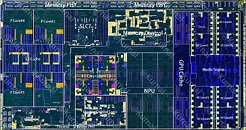
The memory controller and PHY are physically smaller than the one on "Meteor Lake," as it only supports one kind of memory—LPDDR5X. The PHY is cushioned with 8 MB of cache memory, which Intel refers to as memory-side cache.
The NPU takes up a fairly big portion of the central region of the Compute tile. You can make out its six NCEs (neural compute engines), centralized Global Control, and scratchpad RAM. Next to it, is the Xe2 "Battlemage" iGPU, which along with its breakout Display and Media controller components, takes up nearly a third of the Compute tile die-area. It has 8 Xe2 cores, and a large L2 cache memory that's exclusive to the iGPU. Next to the display controllers is Foveros bridge, from which the Compute tile sends high-density microscopic connections to the PCH tile over the base tile.
The 6 nm Platform Controller tile isn't annotated, but it essentially packs USB controllers, display PHY, PCIe root complex, and various other platform I/O.
View at TechPowerUp Main Site | Source
The Kurnalsalts annotation provides a good lay of the land for the Compute tile. The most striking aspect of it is the CPU. "Lunar Lake" comes with a 4P+4E core hybrid CPU, but the two kinds of cores do not share a last-level cache or sit in a ringbus, unlike in case of the Compute tile of "Meteor Lake." The four "Lion Cove" P-cores each come with 2.5 MB of dedicated L2 caches, and share a 12 MB L3 cache. The four "Skymont" E-cores are not part of the ringbus connecting the four P-cores, rather they are physically separated, much like the low-power island E-cores on "Meteor Lake." The E-core cluster shares a 4 MB L2 cache among the four E-cores. This E-core cluster is directly connected to the switching fabric of the Compute tile.


The memory controller and PHY are physically smaller than the one on "Meteor Lake," as it only supports one kind of memory—LPDDR5X. The PHY is cushioned with 8 MB of cache memory, which Intel refers to as memory-side cache.
The NPU takes up a fairly big portion of the central region of the Compute tile. You can make out its six NCEs (neural compute engines), centralized Global Control, and scratchpad RAM. Next to it, is the Xe2 "Battlemage" iGPU, which along with its breakout Display and Media controller components, takes up nearly a third of the Compute tile die-area. It has 8 Xe2 cores, and a large L2 cache memory that's exclusive to the iGPU. Next to the display controllers is Foveros bridge, from which the Compute tile sends high-density microscopic connections to the PCH tile over the base tile.
The 6 nm Platform Controller tile isn't annotated, but it essentially packs USB controllers, display PHY, PCIe root complex, and various other platform I/O.
View at TechPowerUp Main Site | Source

