• Welcome to TechPowerUp Forums, Guest! Please check out our forum guidelines for info related to our community.

Ivy Bridge Die Layout Estimated

btarunr

Editor & Senior Moderator
Staff member
Joined
Oct 9, 2007
Messages
47,876 (7.38/day)
Location
Dublin, Ireland
System Name RBMK-1000
Processor AMD Ryzen 7 5700G
Motherboard Gigabyte B550 AORUS Elite V2
Cooling DeepCool Gammax L240 V2
Memory 2x 16GB DDR4-3200
Video Card(s) Galax RTX 4070 Ti EX
Storage Samsung 990 1TB
Display(s) BenQ 1440p 60 Hz 27-inch
Case Corsair Carbide 100R
Audio Device(s) ASUS SupremeFX S1220A
Power Supply Cooler Master MWE Gold 650W
Mouse ASUS ROG Strix Impact
Keyboard Gamdias Hermes E2
Software Windows 11 Pro
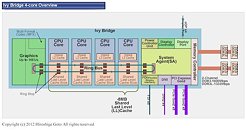
Hiroshige Goto, contributor for PC Watch that is known for detailed schematics of dies estimated the layout of Ivy Bridge silicon. Ivy Bridge is Intel's brand new multi-core processor silicon built on its new 22 nanometer silicon fabrication process. The four core silicon, which four configurations can be carved, will be built into packages that are pin-compatible with today's Sandy Bridge processors. The die area of Ivy Bridge is 160 mm², it has a total transistor count of 1.48 billion, compared to the Sandy Bridge silicon, which has 1.16 billion transistors crammed into a die 216 mm² in area, built on the 32 nm process.

Ivy Bridge has essentially the same layout as Sandy Bridge. The central portion of the die has four x86-64 cores with 256 KB dedicated L2 cache each, and a shared 8 MB L3 cache, while either sides of the central portion has the system agent and the graphics core. All components are bound by a ring-bus, that transports tagged data between the four CPU cores, the graphics core, the L3 cache, and the system agent, which has interfaces for the dual-channel DDR3 integrated memory controller, the PCI-Express controller, and the DMI chipset bus.


Intel can carve four main configurations out of this silicon:
  • 4+2: All four cores enabled, full 8 MB L3 cache enabled, all 16 shader cores (EUs) of the IGP enabled
  • 4+1: All four cores enabled, 6 MB L3 cache enabled, fewer shader cores of the IGP enabled
  • 2+2: Two cores enabled, 4 MB L3 cache enabled, all 16 shader cores of the IGP enabled
  • 2+1: Two cores enabled, 3 MB L3 cache enabled, fewer shader cores of the IGP enabled


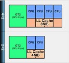
As mentioned earlier, all components on the silicon are bound by a ring-bus that transports data and instructions between the components. This bus has "ring-stops" from where it picks up and drops off data. The graphics core packs up to 16 programmable EUs that handle parallel processing loads for the GPU, they can also be programmed to perform GPGPU tasks. The system agent holds a dual-channel DDR3 integrated memory controller (IMC), a PCI-Express interface that gives out two x8 ports that can work as a single PCI-Express x16, or switched as two x8 ports; a DMI link to the PCH, a display controller, and FDI link to the PCH. Overall, Intel managed to make more efficient use of its die space.


View at TechPowerUp Main Site
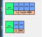
 
160mm^2 for a quad core with HT and IGP.

INTEL's profit margins to hit a new high this year
 
1/3rd of the die area is taken by the crappy GPU cores. What a waste of good silicon:shadedshu
 
With a quad-core die taking only 160mm^2, I wonder how making native dual-core die even makes sense anymore. Will a dual-core version of Haswell exist or will that only be 4+ cores?
 
LMAO. There will be a time when the GPU will take up more space than all the other cores + associated logic combined. At least Intel is rapidly improving their GPU, especially in video display.
 
I like the dead space part on sandy bridge :p.
 
LMAO. There will be a time when the GPU will take up more space than all the other cores + associated logic combined. At least Intel is rapidly improving their GPU, especially in video display.

Rapidly improving? 16 shader cores and add on DX11 support is rapid improvement? Nah they are on par, frantically trying to catch up, but Intel obviously can't pull competitive GPU tech out of their butts very quickly. Not to mention drivers. They have to nail it on both hardware and software fronts...covering years of development by both NV and ATI.

Now the GPU eventually taking up more space...yeah I can see that coming as CPUs and GPU tech merge even more.
 
Rapidly improving? 16 shader cores and add on DX11 support is rapid improvement? Nah they are on par, frantically trying to catch up, but Intel obviously can't pull competitive GPU tech out of their butts very quickly. Not to mention drivers. They have to nail it on both hardware and software fronts...covering years of development by both NV and ATI.
.

Ivy bridge GPU is much better than what you think
http://www.techpowerup.com/160895/C...e-i5-2500K-36-Slower-Than-GeForce-GT-240.html

And shader count doesn't mean anything when you compare different architectures.
 
Still, I dont see why they bother for the upper mainstream processors. why waste all that space that could go toward more cache or something. considering $30 graphics cards out perform Intel IB IGP, the only thing I can think the IGP would be handy for is ITX/media or workstations, neither which even need a top end ivy bridge processor.
 
There are some oddities in the slides that i'd like to bring to attention:

1) in the IB layour schematic(165d), the PCIe lanes say "gen2", since IB is gen3, why is that?
2) this is more of a design oddity that i can't make sense of compared to SB: why are the display outputs on the SA(FDI, eDP, DAC) furthest from the graphics core?.
i mean, when you're processing graphics/video decode, now the data first has to go through the ring to the GPU, THEN COME BACK through the entire ring back to the SA to be outputted?.
My deduction on that design call is that once the data is processed and in the (main ram) framebuffer then it makes sense to have the display outputs on the SA side as they'd only need to access the ram address space -which is in the same SA so not neededing a full ring access-...
if it where on the GPU side like SB, then you'd need 3 ring accesses, once to get data to the gpu, another to put data in framebuffer and another to readback the framebuffer to display outputs.
 
Still, I dont see why they bother for the upper mainstream processors. why waste all that space that could go toward more cache or something. considering $30 graphics cards out perform Intel IB IGP, the only thing I can think the IGP would be handy for is ITX/media or workstations, neither which even need a top end ivy bridge processor.

In newegg I can't find any $30 graphics that can match IB IGP

Intel HD4000 should be much better than Nvidia 8400GS and ATI HD5450, and those are the only ones that cost around ~ $30

And for laptops, the price of equivalent dedicated GPU is even higher.
 
Where is Ivy Bridge-E specs!
 
Oh good atleast I have some time to enjoy my SB-E, I was worried that by the time this thing ships out 28th Ivy bridge would be out.
 
so are all next gen Intel CPUs going to have a GPU core?
 
so are all next gen Intel CPUs going to have a GPU core?
I believe the only versions that will not have a GPU core is the high end models such as the SandyBridges. Also shader count means jack, it all has to do with efficiency.

An In-efficient 100 shaders would get blown away by 50 efficient shaders.
 
all current-gen(and since the last gen too) have integrated GPU, so yes, moving forward it's going to integrate even more stuff, i'm sure the future will look more like a SoC with standard bus peripherals for added functionality(pcie adapters/switches, usb, etc).

SNB already has eDP onboard, the next step would be to directly forego the FDI and have all -digital- display outputs(i think the fdi is there for DVI and HDMI and analog VGA), a single/dual DP output.

BTW: they might release non-GPU(or actually, gpu silicon laser-disabled at the fab) versions like they currently do with normal SNB.
And apart from SNB-E that doesn't has onboard gpu, the entire Xeon line won't have integrated gpu either
 
With a quad-core die taking only 160mm^2, I wonder how making native dual-core die even makes sense anymore. Will a dual-core version of Haswell exist or will that only be 4+ cores?

Keep in mind that the Wolfdale die with 6MB of L2 cache was 107 mm2, and the Wolfdale-3M die with 3MB of L2 was only 82 mm2. The integration of memory controller PCI-Express controllers and a GPU have really added to die sizes.

The Ivy Bridge dual core die with 4MB L3 and HD4000 graphics will be approximately 118mm2. Despite a two node manufacturing advantage, Ivy Bridge dual cores are still larger than Wolfdale. There will probably also be another Ivy dual core die with 3MB L3 and HD 2500 with a die size below 100 mm2.

Given that Haswell is still on 22nm, has a larger GPU than Ivy, and supposedly has 1MB L2 cache per core (vs 256k), I expect there will still be native dual core dies.
 
Back
Top