• Welcome to TechPowerUp Forums, Guest! Please check out our forum guidelines for info related to our community.
  • The forums have been upgraded with support for dark mode. By default it will follow the setting on your system/browser. You may override it by scrolling to the end of the page and clicking the gears icon.

AMD Zen 2 "Rome" MCM Pictured Up Close

btarunr

Editor & Senior Moderator
Staff member
Joined
Oct 9, 2007
Messages
47,849 (7.39/day)
Location
Dublin, Ireland
System Name RBMK-1000
Processor AMD Ryzen 7 5700G
Motherboard Gigabyte B550 AORUS Elite V2
Cooling DeepCool Gammax L240 V2
Memory 2x 16GB DDR4-3200
Video Card(s) Galax RTX 4070 Ti EX
Storage Samsung 990 1TB
Display(s) BenQ 1440p 60 Hz 27-inch
Case Corsair Carbide 100R
Audio Device(s) ASUS SupremeFX S1220A
Power Supply Cooler Master MWE Gold 650W
Mouse ASUS ROG Strix Impact
Keyboard Gamdias Hermes E2
Software Windows 11 Pro
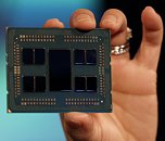
Here is the clearest picture of AMD "Rome," codename for the company's next-generation EPYC socket SP3r2 processor, which is a multi-chip module of 9 chiplets (up from four). While first-generation EPYC MCMs (and Ryzen Threadripper) were essentially "4P-on-a-stick," the new "Rome" MCM takes the concept further, by introducing a new centralized uncore component called the I/O die. Up to eight 7 nm "Zen 2" CPU dies surround this large 14 nm die, and connect to it via substrate, using InfinityFabric, without needing a silicon interposer. Each CPU chiplet features 8 cores, and hence we have 64 cores in total.

The CPU dies themselves are significantly smaller than current-generation "Zeppelin" dies, although looking at their size, we're not sure if they're packing disabled integrated memory controllers or PCIe roots anymore. While the transition to 7 nm can be expected to significantly reduce die size, groups of two dies appear to be making up the die-area of a single "Zeppelin." It's possible that the CPU chiplets in "Rome" physically lack an integrated northbridge and southbridge, and only feature a broad InfinityFabric interface. The I/O die handles memory, PCIe, and southbridge functions, featuring an 8-channel DDR4 memory interface that's as monolithic as Intel's implementations, a PCI-Express gen 4.0 root-complex, and other I/O.


View at TechPowerUp Main Site
 
Will Rome be using dies from both TSMC(7 nm chiplets) and GF(14 nm I/O) right?
Also will less than 64 cores CPUs be using dummy or faulty silicon as before?
Also will the 2 dies next to each other communicate directly?
I don't think Ryzen 3000 will use the I/O die, since it is 14 nm and is huge and perhaps very expensive. That means that Rome either has IMC and PCI disabled, or more likely Ryzen will have a different die.
 
AMD has been looking at no NB for Ryzen 2 3000 Series
 
I hope the memory latency is indeed reduced. As I see it right now instead of a worst case of 2 'hops' to memory on the current models it will now ALWAYS have two hops. I was expecting a silicon interposer like on Vega which would have better performance.
 
Will Rome be using dies from both TSMC(7 nm chiplets) and GF(14 nm I/O) right?
Also will less than 64 cores CPUs be using dummy or faulty silicon as before?
Also will the 2 dies next to each other communicate directly?
I don't think Ryzen 3000 will use the I/O die, since it is 14 nm and is huge and perhaps very expensive. That means that Rome either has IMC and PCI disabled, or more likely Ryzen will have a different die.

This is straight out of my a**, but there could be a smaller I/O die with four IF links, 2-channel DDR4, 32-lane PCIe gen 4.0, etc. If AMD uses two 8-core chiplets with that die, it could achieve 16-core/32-thread on the AM4 package.

So the performance of a 2950X in the MSDT segment could hurt Intel plenty.
I do not expect a 16 core for less than 700 dollars, so it wont be in the mainstream, even if is AM4. Anyway the mainstream user do not need more than 8 cores.
 
Also looking at the die sizes of those 8-core chiplets, a monolithic 16-core Zen 2 die with fully integrated NB+SB won't be much bigger than a Zeppelin.
 
Still relevant:
more-cores.png
 
I don't know what AMD is planning with Ryzen 3xxx on the CPU side, but I have some insight on the chipset side of things.

First the bad news, motherboards are going to get even more expensive, as with PCIe 4.0 the boards are going to need some kind of "re-driver" for the PCIe 4.0 signals and apparently at least one is required, but if you want dual x16 slots on boards, supposedly two are needed. These are expensive parts and will increase board costs.

From my understanding, AMD is going full-on PCIe 4.0, so not only the lanes from the CPU to the chipset will be PCIe 4.0, but also the lanes to all peripherals. This means AMD will be the first company to offer full PCIe 4.0 support on a consumer board, unless Intel can get something out before the Ryzen 3xxx series launches. Expect a vastly improved chipset, but I can't reveal too much as yet, as I don't want to get people in trouble for leaking information that isn't even remotely public as yet. All I can say is that I think everyone will be a lot happier with AMD's high-end chipset for the Ryzen 3xxx series, as it doesn't have any of the weird limitations that the current chipsets have. There won't be any bandwidth starved peripherals this time around.
 
So it looks like the CPUs are gradually transforming into GPUs or Stream Processors.
Not bad, however the software is ridiculously overly-behind for multi core able applications, and I am not talking only about Game Engines.
 
it's absolutely amazing what AMD did in just 1.5 years
intel did nothing in 10 yrs

that cpu looks so beautiful
 
Last edited:
I do not expect a 16 core for less than 700 dollars, so it wont be in the mainstream, even if is AM4. Anyway the mainstream user do not need more than 8 cores.
Try $500 at least for the lower clock variants, a mainstream AM4 part won't exceed that unless AMD meets all expectations & gets max core (Over)clock to reach 5Ghz. Of course we don't know if the 16 core (IGP less) variant will be mainstream or not, so we'll have to wait a bit till the desktop parts are confirmed.
 
Last edited:
it's absolutely amazing what AMD did in just 1.5 years
intel did nothing in 10 yrs

that cpu looks so beautiful

You assume too much. Intel has made gobs of headway in multiple markets. Just because they aren't something you look for doesn't mean they don't exist. The knights landing projects are an example of this. I am excited for AMD finally doing things. This looks like a fix for the current memory limitations facing the 2990wx however it makes it obvious a new socket will be needed. Time will tell what the cost effectiveness of this will be. I hope that we do see a new socket for MDT as well addressing the huge limitations on those.
 
You assume too much. Intel has made gobs of headway in multiple markets. Just because they aren't something you look for doesn't mean they don't exist. The knights landing projects are an example of this. I am excited for AMD finally doing things. This looks like a fix for the current memory limitations facing the 2990wx however it makes it obvious a new socket will be needed. Time will tell what the cost effectiveness of this will be. I hope that we do see a new socket for MDT as well addressing the huge limitations on those.

i don't care about other projects, my dear friend, all i care about are CPUs and GPUs
because of the past 10 yrs and intel's "good consumer policies", i just hate them, truly hate them

PS: let's not forget how and what intel did to AMD for reaching a now shaking 1 position
 
Judging from the die size, I'd say there is a high probability that L3 cache is present on individual CPU chiplet.

Despite that AMD didn't clarify its FPU architecture, THIS IS F**KING AWESOME. Threadripper 3000s will be perfect for HPC.
 
Judging from the die size, I'd say there is a high probability that L3 cache is present on individual CPU chiplet.

Despite that AMD didn't clarify its FPU architecture, THIS IS F**KING AWESOME. Threadripper 3000s will be perfect for HPC.
This might shead some light on the FPU.
ZEN2_5.jpg
 
Judging from the die size, I'd say there is a high probability that L3 cache is present on individual CPU chiplet.

Despite that AMD didn't clarify its FPU architecture, THIS IS F**KING AWESOME. Threadripper 3000s will be perfect for HPC.

Do you think they put a large L4 cache on the center IO chip?
 
This might shead some light on the FPU.
From both what they said and what is on the slides it looks like Zen2 will have proper AVX. Except they are doing their best to avoid saying that out loud and resort to marketingspeak :D

IO Hub will inevitably increase memory latency as no CPU chiplets will have direct access to memory. AMD's wording was quite clever, they said someting along the lines of no more variable RAM access latency :). This does not look right for the desktop/gaming CPU especially if the competition keeps going the current way. Does desktop even need more than 8 cores at this point?
 
This is just great. if IPC is 10% over Zen+, Intel should really really be afraid of their sales in the next couple of years.
 
however it makes it obvious a new socket will be needed.
AMD stated plainly that Rome is socket compatible with previous-gen EPYC. So no, no new socket needed. Why would it be?


As for consumer facing chips, this looks absolutely brilliant. Why? Because of the innate scalability and flexibility of this design. They still have the "one die to rule them all" design, only now it's one 8-core CCX. No more inter-core IF at 8 cores or less. No more inter-CCX latencies or other issues at or below 8 cores, which is plenty for >99% of consumers. As for the I/O die, they can make however many designs they want, and they'll be relatively cheap Lego-like designs. X number of IF ports, Y DRAM channels, various other I/O blocks, cut, paste, done, fab. On a proven and well known process node from a supplier where they have plentiful capacity and favorable pricing. This will let AMD diversify their product portfolio while maintaining fab/die portfolio simplicity for the complex logic dice. Ryzen gets a small I/O die with dual channel memory, < 32 PCIe lanes and support for up to two active dice. This could be very small, given the dramatic reduction in I/O needs from EPYC. TR gets four active dice, quad channel, 64 PCIe, at half the size of the full-fat EPYC I/O chip (or less, given there's no need for IF for multi-socket platforms). APUs could either re-use the Ryzen one, just replacing one die with a GPU over IF, or get a bespoke solution with different I/O. Mobile could get a tiny I/O die with just the basics (a couple of SATA, 4-ish USB, video output, 8-16 PCIe).

My only real concern here is the cost and complexity of implementing an mcm design on smaller packages, given how thick and massive TR4 packages and substrates are, but then again, linking 2-3 dice with short and straight runs of IF should be far simpler than the 4-way crosswise layout of Threadripper. At least outside of mobile, this should be entirely doable (at now that we see that they can do 9 dice on a single substrate in TR4).

As for memory latency, it'll obviously increase compared to having the DRAM controller on-die, but the increase ought to be smaller than current TR/EPYC die-to-die hops given that the die with the DRAM controllers now only does I/O, and should have a far more optimized layout for this. This isn't ideal, but likely not a performance killer either. Given that they say their memory controllers are quite improved, it'll likely be a wash for consumer use cases.

Add to this what looks like a significant IPC increase in a wide swath of applications, clock speed increases (1.25x at same power according to the slides, so 8 cores at 4.5GHz (3.6GHz*1.25) at 95W if we're going off the 1800x. This sounds quite optimistic, but given how badly GloFo 14nm scaled above 4GHz, it might be possible. If we get 3-4-core turbo above 4.5GHz, that'd be an amazing gaming chip.


My main question now is whether AMD is able to attach HMB2 to an APU in this same way, or if that still requires an interposer/EMIB. I'm skeptical of this being possible, but if it is - hot damn, next-gen APUs could be amazing.
 
now it's one 8-core CCX. No more inter-core IF at 8 cores or less.
Do we have confirmation on this? As fas as I have seen, there have not been any details about the internals of Zen2.
 
I like that AMD has caught up to AMD but i'm starting getting afraid AMD may have surpassed it. They seem to have so by quite a margin, based on this presentation, in the server space but we have yet to see it in the desktop space.

Why i'm afraid? If AMD does end ahead of Intel, what's to stop AMD from pricing their chips like Intel?
 
Get that into consumer space already. The tinkerer in me has been asleep ever since Sandy Bridge. So, AMD: go ahead, make my day!
 
Back
Top