• Welcome to TechPowerUp Forums, Guest! Please check out our forum guidelines for info related to our community.
  • The forums have been upgraded with support for dark mode. By default it will follow the setting on your system/browser. You may override it by scrolling to the end of the page and clicking the gears icon.

AMD RDNA2 Graphics Architecture Detailed, Offers +50% Perf-per-Watt over RDNA

Glad you jumped off the 'because they are worried' boat!

The waiting to finalize clocks/specs is quite normal. But it's not like they are sitting there ready to go waiting on amd to release. They, naturally, are not ready.
Here is the exact Source which is why I originally said Nvidia may be worried or something. Which they are not.

Nvidia is supposingly getting a little nervous but then states not in terms of being worried, but because Nvidia may have to alter its next gen GPU specifications as to ensure they have enough to combat the Big Navi GPU.
At the TIME 3:17 or listen to 3:00 to 4:00 about a minute.
 
I have to say that (without having done the numbers very thoroughly) the XSX APU makes it seem like AMD have managed some significant density gains with RDNA 2 on the tweaked 7nm node. Navi 10 is 251mm² and 40CUs. The XSX APU is 360mm² nd 56CUs (52 in use to reduce discard rates). Discounting everything else that sounds like similar density 6.3 vs. 6.4mm² per CU), but the XSX APU also has a full 8-core Zen2 CPU in there, which eats a significant portion of that die area. Sure, it likely cuts down on a lot of PC-centric stuff (less I/O etc.) but not by much, and not enough to really matter. It also had RT hardware in there.

Makes me rather curious to see the sizes of RDNA2 GPUs for PC.

505 sq.mm. https://www.ptt.cc/bbs/PC_Shopping/M.1577766534.A.08E.html
 
That's not a source, you can just right-click your mouse button and translate the original link to any language you want.
But that linked you posted cited the link I posted.
 
English source
Beyond this being a random post on a random BBS with zero reason for us to believe it ("According to people familiar with the matter at the Taiwan PTT Forum", lol), and some very questionable assertions ("It was also pointed out that given the huge Die size of the GPU itself, the card will eventually not use HBM, but instead rely on GDDR6 " - yet this die is reportedly significantly smaller than Fiji, which used HBM, and there's no reason two stacks of HBM2(E) wouldn't fit just fine next to a 505mm² die). Also, there's nothing new in that rumor, it's been rehashed over and over and over again on these forums and elsewhere. Still, let's be generous and assume it's somewhat accurate. The question then becomes: 505mm2 of what?

The density gains of the XSX would indicate more than 1:1 scaling from Navi 10, i.e. a 505mm2 chip would either have >80 CUs or some other stuff added on that we don't yet know about. Let's look closer at this.

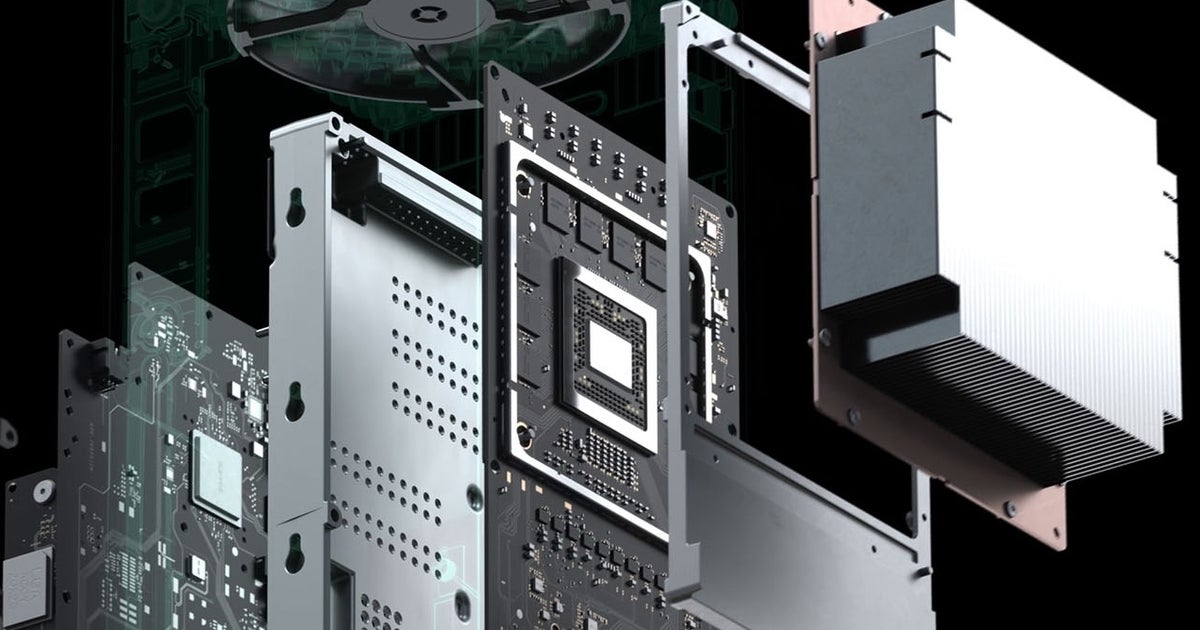
Navi 10 has 40 CUs, a 256-bit G6 bus and a single IF/PCIe 4.0 x16 link on a 251mm² die. The XSX die is 360mm² with 56 CUs, 8 Zen 2 cores, and I/O including a 320-bit G6 bus. A Zen 2 CCD is 74 mm² with two 31.3 mm² CCXes, 16MB of L3, IF links and anything else that lives on that die. Let's be conservative and discount L3 completely - the XSX then uses at least 2x31.3 mm² = 62.6mm² of die area to its CPU cores (likely a bit more as it won't have zero L3 cache, but will also likely gain density from the node improvement. Some space will also be used for the IF links between the CPU, GPU and memory controllers). This leaves us with at most 360mm² - 63mm² = 297mm² for 52 56 CUs, all encode/decode blocks (which given the importance of streaming are likely to be fully featured and not cut down), a 320-bit GDDR6 PHY + controllers (compared to the 256-bit PHY and controllers of Navi 10, so 25% more die area for that), and at least two PCIe links for SSDs (unknown whether these are PCIe 3.0x4, PCIe 4.0x2 or PCIe 4.0x4 at this point), plus the chipset uplink etc. While the XSX does gain something in having slightly less I/O than a PC GPU, the gains from that are minor at best. Ignoring that, we have a 25% increase in VRAM die area + a 30% 40% increase in CUs with just an ~18% increase in die size (with the CPU subtracted, that is). And that includes RT hardware.

While this is some real napkin math (we have no idea if anything beyond the die sizes here is actually accurate in terms of numbers, but IMO they shouldn't be too far off), it tells us that a 505mm² RDNA 2 GPU on the same improved 7nm node as the XSX either must have more than 80 CUs - if the scaling roughly follows my calculations a 100% area increase would then be more like a 120% increase in CUs, or ~95 CUs - or use a lot of die area for something else. Might we see significantly more RT power compared to shader pwerformance in the PC GPUs? Also, if it uses HBM2 rather than a stupidly large 512-bit G6 bus (which IMO sounds likely, despite what that BBS post says), the CU count could grow further (100?) as HBM controllers and PHYs are much more space efficient than G6.

Still, with all of this within the realm of IMO reasonable speculation (and it is very much speculation at this point) we have no idea about power, clocks, or anything else. Performance would vary wildly based on all of this. Pricing is also crucial, and a 505mm2 die on TSMC 7nm is not going to be cheap. So, as I've said both here and elsewhere, I don't see a reason to doubt that AMD can bring about a true flagship this generation, but both the absolute performance and pricing is entirely up in the air at this point, as is its competitiveness with Nvidia's so far entirely unknown Ampere arch. There's absolutely no indication in any of this that this will beat Ampere, simply because Ampere is entirely unknown. But will it be powerful? Absolutely.


Edit: I borked my numbers from about halfway through by calculating from the 52 active CUs in the XSX die rather than the 56 physically present ones. Fixed that; also added a note about possibly using "free" die space for more RT power compared to consoles.
 
Last edited:
The RT hardware is very important. RTX 2080 Ti can do 10 Giga Rays of ray tracing performance and 78 trillion RTX-OPS.

I am quite sure that IF AMD wants to be competitive, they will design the Navi 2 GPU to be in line performance-wise with what comes next after Turing.
I mean it should be easy for them to take all the data they can gather on the previous generations and calculate an appropriate performance window range where the Turing successor will likely fall.

They did it with Zen. And they said that Zen targets the performance level where they expected Skylake-next-gen to be.
That, my friend, is what is called an estimate. Which for all intents and purposes is a qualified guess. A single event in the real world will likely fall within a certain margin of a statistical estimate, but it might well not, as statistics are a post hoc phenomenon; they only chart what has happened and can be used to estimate (i.e. guess) what will happen in the future. An estimate can be 100% correct or wildly inaccurate, there's no way of knowing until the thing being estimated becomes a reality. Generational GPU performance increases have been anywhere from near nothing to revolutionary, and there really isn't any reliable way of knowing which one is coming next.

I mean, sure, AMD has obviously been working on their next flagship GPU based on an estimate of where Nvidia's competing architecture will be in terms of performance. But so what? They're still going to make the best products they can within the constraints of die size/cost/power/thermals for the high end, with everything else being spaced downwards to be competitive while producing sufficient margins and selling well. Only pricing (and thus margins) and the specifics of cut-down SKUs is really dependent on the competition.
 
The RT hardware is very important. RTX 2080 Ti can do 10 Giga Rays of ray tracing performance and 78 trillion RTX-OPS.

I am quite sure that IF AMD wants to be competitive, they will design the Navi 2 GPU to be in line performance-wise with what comes next after Turing.
I mean it should be easy for them to take all the data they can gather on the previous generations and calculate an appropriate performance window range where the Turing successor will likely fall.

They did it with Zen. And they said that Zen targets the performance level where they expected Skylake-next-gen to be.

Nah, that has to be a typo. 78 billion, not trillion.
The next-gen XBox will do 380 billion:
"the hardware acceleration for ray tracing maps traversal and intersection of light at a rate of up to 380 billion intersections per second"

Specs (all clocks are fixed, silicon is custom):
  • 12.155 TFLOPs
  • AMD Zen 2 8c/16t @ 3.6-3.8 Ghz - Hyperthreading can be disabled for a 3.8 Ghz clock or enabled for a 3.6 ghz clock
  • 16 GB GDDR6 ECC (!!!)
  • 52 CU 3328 Shader GPU @ 1,825 MHz
  • Memory bandwidth: 10GB at 560GB/s, 6GB at 336GB/s
  • 7nm - NOT EUV
  • 1TB NVME SSD storage
 
Don't need 7nm EUV, the enhanced 7nm version is more than enough and efficient.
 
Don't need 7nm EUV, the enhanced 7nm version is more than enough and efficient.
Here is to hoping that is true... depends on where they tweak these, eh? I mean 5500 XT and 5700 XT aren't winning power /performance, but the 5600 XT is matching it...

... and Nvidia is still on 12nm.
 
Here is to hoping that is true... depends on where they tweak these, eh? I mean 5500 XT and 5700 XT aren't winning power /performance, but the 5600 XT is matching it...

... and Nvidia is still on 12nm.
I'm only going by AMDs explanation on why they changed the roadmaps from 7nm+ to just 7nm. They said it's an enhanced refined 7nm in comparison to the 5700XT 7nm process node.
The 5700XT is based on RDNA1. The upcoming RDNA2 is far more efficient. The XboxSX shows how efficient and fast it is, and that's a limited sample size APU. Lol

Nvidia should see a massive efficiency lift from 12nm all the way down to 7nm and some claim even 10nm and 8nm.

 
Last edited:
I'm only going by AMDs explanation on why they changed the roadmaps from 7nm+ to just 7nm. They said it's an enhanced refined 7nm in comparison to the 5700XT 7nm process node.
The 5700XT is based on RDNA1. The upcoming RDNA2 is far more efficient. The XboxSX shows how efficient and fast it is, and that's a limited sample size APU. Lol

Nvidia should see a massive efficiency lift from 12nm all the way down to 7nm and some claim even 10nm and 8nm.

Your unfettered optimism over AMD never ceases. :)
 
Your unfettered optimism over AMD never ceases. :)
Intel and Nvidia can afford to fall behind. AMD cannot. But I'm optimistic because of the XSX specs.
 
You were optimistic from silly rumors already! :)
Everything starts from a rumor in this industry. Plus I already knew that RDNA2 was going to be a "Major" difference and have "Major" efficiency gains in comparison to GCN. Most industry sources even dating back to 2018 already knew this, despite being a rumor or speculation.

I'm sure you already knew this too. It's all about Next Generation Gaming Consoles.
 
Plus I already knew that RDNA2 was going to be a "Major" difference and have "Major" efficiency gains in comparison to GCN.
It fookn better... that was 2 generations ago........lolololol...useless talking point, man. You seem to still expect a node shrink + arch update results from a simple arch update...

I bet it REALLY has more efficiency than the generation before that too!!! lol
 
Nah, that has to be a typo. 78 billion, not trillion.
The next-gen XBox will do 380 billion:
"the hardware acceleration for ray tracing maps traversal and intersection of light at a rate of up to 380 billion intersections per second"

Specs (all clocks are fixed, silicon is custom):
  • 12.155 TFLOPs
  • AMD Zen 2 8c/16t @ 3.6-3.8 Ghz - Hyperthreading can be disabled for a 3.8 Ghz clock or enabled for a 3.6 ghz clock
  • 16 GB GDDR6 ECC (!!!)
  • 52 CU 3328 Shader GPU @ 1,825 MHz
  • Memory bandwidth: 10GB at 560GB/s, 6GB at 336GB/s
  • 7nm - NOT EUV
  • 1TB NVME SSD storage

It's 78 RTX Ops. No billion, no trillion, not even thousand.

 
How does this 10 GRays/s and 78 RTX Ops compare to Xbox's 380 billion I/s?

It's very difficult to compare those numbers, as even though they can quote the same scale, it's calculated differently per generation. Two different generations of GPU can be quoted for the same basic TFLOP output, but the newest one can be 30% faster in everything than the previous generation.
 
It fookn better... that was 2 generations ago........lolololol...useless talking point, man. You seem to still expect a node shrink + arch update results from a simple arch update...

I bet it REALLY has more efficiency than the generation before that too!!! lol
Are you assuming that RDNA2 is a very minor RDNA1 update? If you are then that's a LMAO to you.

According to sources and AMD themselves, RDNA2 is a architecture overhaul. What does Nvidia's GPU architecture have to do with RDNA2? Absolutely nothing lol, but you seem to be a little confused or too Nvidia biased. To each there own I suppose. I'll follow the evidence, you can continue to follow the fantasies.
lol, no... weve went over this already...what are you not comprehending? Are you losing something in translation now?

Lol fantasies...lolololwtfbbqfanboysos
 
lol, no... weve went over this already...what are you not comprehending? Are you losing something in translation now?

Lol fantasies...lolololwtfbbqfanboysos
You are a Nvidia Fanboy. It's OK to like a company over another. Congratulations,
 
You are a Nvidia Fanboy. It's OK to like a company over another. Congratulations,
I'm not at all. Nothing I've said even infers such a thing. Look at my previous posts! I used the same information you did, but others here are talking your points down off a ledge, not mine. I play both sides to middle...my posts support that. Your highly optimistic opinion is the one rooted in rumor and assumption. I have no expectations of this product outside of it being competitive.

It's like groundhog day with you, lol.
 
Last edited:
Back
Top