- Joined
- Oct 9, 2007
- Messages
- 47,685 (7.42/day)
- Location
- Dublin, Ireland
| System Name | RBMK-1000 |
|---|---|
| Processor | AMD Ryzen 7 5700G |
| Motherboard | Gigabyte B550 AORUS Elite V2 |
| Cooling | DeepCool Gammax L240 V2 |
| Memory | 2x 16GB DDR4-3200 |
| Video Card(s) | Galax RTX 4070 Ti EX |
| Storage | Samsung 990 1TB |
| Display(s) | BenQ 1440p 60 Hz 27-inch |
| Case | Corsair Carbide 100R |
| Audio Device(s) | ASUS SupremeFX S1220A |
| Power Supply | Cooler Master MWE Gold 650W |
| Mouse | ASUS ROG Strix Impact |
| Keyboard | Gamdias Hermes E2 |
| Software | Windows 11 Pro |
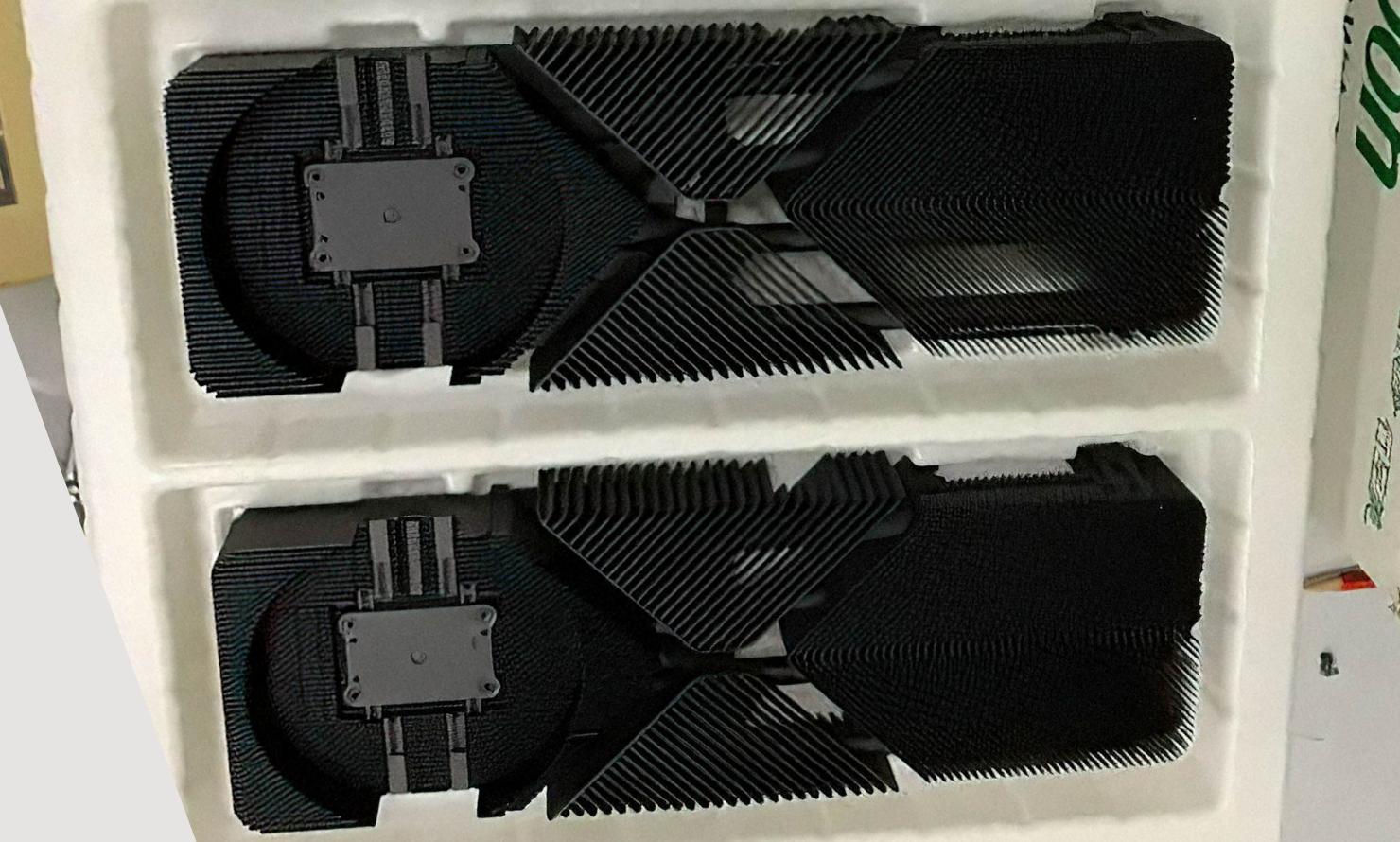
NVIDIA's next-generation GeForce "Ampere" RTX 3000 series graphics cards are heading for a September reveal, along with availability shortly after. Much of the news cycle over the past couple of weeks revolved around alleged leaks of the card's cooling solution that provides insights into what the finished product could look like, with some even doubting the veracity of the picture leaks given the September launch. Igor's Lab did some digging into the production timeline of these cards. The leaks seem to perfectly align with the timeline.
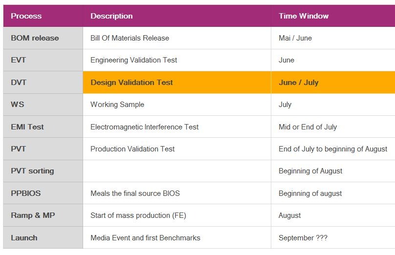
The chip design, prototyping, taping-out, and testing of "Ampere" IP completed before the mass-production timeline kicks off. This begins in April/May, with NVIDIA's OEM partners and other suppliers finalizing a bill of materials (BOM). June is also when the products go through the EVT (engineering validation test) and DVT (design validation test). It is at these stages that NVIDIA has the opportunity to approve or summarily reject/change the design of the product and finalize it. By July, there are working samples of the finished products for NVIDIA and its industry partners to validate. This is also when regulators such as the FCC and CE conduct EMI tests. Production validation tests (PVT), or proofing of the production line, occurs in late-July/early-August. The final BIOS is released to the OEM by NVIDIA around this time. Mass-production finally commences in August, and the onward march to distributors rolls on. The media event announcing the product and press reviews follow in September, and market availability shortly thereafter.

View at TechPowerUp Main Site
The chip design, prototyping, taping-out, and testing of "Ampere" IP completed before the mass-production timeline kicks off. This begins in April/May, with NVIDIA's OEM partners and other suppliers finalizing a bill of materials (BOM). June is also when the products go through the EVT (engineering validation test) and DVT (design validation test). It is at these stages that NVIDIA has the opportunity to approve or summarily reject/change the design of the product and finalize it. By July, there are working samples of the finished products for NVIDIA and its industry partners to validate. This is also when regulators such as the FCC and CE conduct EMI tests. Production validation tests (PVT), or proofing of the production line, occurs in late-July/early-August. The final BIOS is released to the OEM by NVIDIA around this time. Mass-production finally commences in August, and the onward march to distributors rolls on. The media event announcing the product and press reviews follow in September, and market availability shortly thereafter.
View at TechPowerUp Main Site