• Welcome to TechPowerUp Forums, Guest! Please check out our forum guidelines for info related to our community.

Samsung Leads Semiconductor Paradigm Shift with New Material Discovery

btarunr

Editor & Senior Moderator
Staff member
Joined
Oct 9, 2007
Messages
46,393 (7.67/day)
Location
Hyderabad, India
System Name RBMK-1000
Processor AMD Ryzen 7 5700G
Motherboard ASUS ROG Strix B450-E Gaming
Cooling DeepCool Gammax L240 V2
Memory 2x 8GB G.Skill Sniper X
Video Card(s) Palit GeForce RTX 2080 SUPER GameRock
Storage Western Digital Black NVMe 512GB
Display(s) BenQ 1440p 60 Hz 27-inch
Case Corsair Carbide 100R
Audio Device(s) ASUS SupremeFX S1220A
Power Supply Cooler Master MWE Gold 650W
Mouse ASUS ROG Strix Impact
Keyboard Gamdias Hermes E2
Software Windows 11 Pro
Researchers at the Samsung Advanced Institute of Technology (SAIT) have unveiled the discovery of a new material, called amorphous boron nitride (a-BN), in collaboration with Ulsan National Institute of Science and Technology (UNIST) and the University of Cambridge. Published in the journal Nature, the study has the potential to accelerate the advent of the next generation of semiconductors.

Recently, SAIT has been working on the research and development of two-dimensional (2D) materials - crystalline materials with a single layer of atoms. Specifically, the institute has been working on the research and development of graphene, and has achieved groundbreaking research outcomes in this area such as the development of a new graphene transistor as well as a novel method of producing large-area, single-crystal wafer-scale graphene. In addition to researching and developing graphene, SAIT has been working to accelerate the material's commercialization.


"To enhance the compatibility of graphene with silicon-based semiconductor processes, wafer-scale graphene growth on semiconductor substrates should be implemented at a temperature lower than 400°C." said Hyeon-Jin Shin, a graphene project leader and Principal Researcher at SAIT. "We are also continuously working to expand the applications of graphene beyond semiconductors."

2D Material Transformed - Amorphous Boron Nitride
The newly discovered material, called amorphous boron nitride (a-BN), consists of boron and nitrogen atoms with an amorphous molecule structure. While amorphous boron nitride is derived from white graphene, which includes boron and nitrogen atoms arranged in a hexagonal structure, the molecular structure of a-BN in fact makes it uniquely distinctive from white graphene.

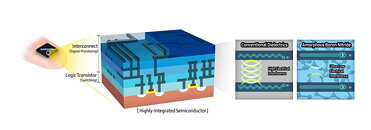
Amorphous boron nitride has a best-in-class ultra-low dielectric constant of 1.78 with strong electrical and mechanical properties, and can be used as an interconnect isolation material to minimize electrical interference. It was also demonstrated that the material can be grown on a wafer scale at a low temperature of just 400°C. Thus, amorphous boron nitride is expected to be widely applied to semiconductors such as DRAM and NAND solutions, and especially in next generation memory solutions for large-scale servers.

"Recently, interest in 2D materials and the new materials derived from them has been increasing. However, there are still many challenges in applying the materials to existing semiconductor processes." said Seongjun Park, Vice President and Head of Inorganic Material Lab, SAIT. "We will continue to develop new materials to lead the semiconductor paradigm shift."

Timeline:
  • 2012: Graphene Barristor, a Triode Device with a Gate-Controlled Schottky Barrier (SAIT, published in Science)
  • 2014: Wafer-Scale Growth of Single-Crystal Monolayer Graphene on Reusable Hydrogen-Terminated Germanium (SAIT and Sungkyunkwan University, published in Science)
  • 2017: Realization of continuous Zachariasen carbon monolayer (SAIT and Sungkyunkwan University, published in Science Advances)
  • 2020: Ultra-low dielectric constant amorphous boron nitride (SAIT, UNIST and University of Cambridge, published in Nature)

View at TechPowerUp Main Site
 
Joined
Feb 18, 2005
Messages
5,238 (0.75/day)
Location
Ikenai borderline!
System Name Firelance.
Processor Threadripper 3960X
Motherboard ROG Strix TRX40-E Gaming
Cooling IceGem 360 + 6x Arctic Cooling P12
Memory 8x 16GB Patriot Viper DDR4-3200 CL16
Video Card(s) MSI GeForce RTX 4060 Ti Ventus 2X OC
Storage 2TB WD SN850X (boot), 4TB Crucial P3 (data)
Display(s) 3x AOC Q32E2N (32" 2560x1440 75Hz)
Case Enthoo Pro II Server Edition (Closed Panel) + 6 fans
Power Supply Fractal Design Ion+ 2 Platinum 760W
Mouse Logitech G602
Keyboard Logitech G613
Software Windows 10 Professional x64
Congratulations to these researchers for continuing to push the envelope and further the pursuit of knowledge.

The only issue, of course, is how much this will cost to manufacture and how long the lead time to market will be. The fact that we don't have any type of graphene products in commercial production today suggests it will sadly be a long time before we see a-BN semiconductors in our PCs.
 

TheLostSwede

News Editor
Joined
Nov 11, 2004
Messages
16,075 (2.26/day)
Location
Sweden
System Name Overlord Mk MLI
Processor AMD Ryzen 7 7800X3D
Motherboard Gigabyte X670E Aorus Master
Cooling Noctua NH-D15 SE with offsets
Memory 32GB Team T-Create Expert DDR5 6000 MHz @ CL30-34-34-68
Video Card(s) Gainward GeForce RTX 4080 Phantom GS
Storage 1TB Solidigm P44 Pro, 2 TB Corsair MP600 Pro, 2TB Kingston KC3000
Display(s) Acer XV272K LVbmiipruzx 4K@160Hz
Case Fractal Design Torrent Compact
Audio Device(s) Corsair Virtuoso SE
Power Supply be quiet! Pure Power 12 M 850 W
Mouse Logitech G502 Lightspeed
Keyboard Corsair K70 Max
Software Windows 10 Pro
Benchmark Scores https://valid.x86.fr/5za05v
Congratulations to these researchers for continuing to push the envelope and further the pursuit of knowledge.

The only issue, of course, is how much this will cost to manufacture and how long the lead time to market will be. The fact that we don't have any type of graphene products in commercial production today suggests it will sadly be a long time before we see a-BN semiconductors in our PCs.

Not true, there are graphene speaker elements. If you only meant semiconductors, then no, none that I know of at least.
 
Joined
Mar 13, 2012
Messages
277 (0.06/day)
It is all just getting ridiculous, massive amount of money poured in to R&D finding all these amazing materials that ends up in nothing.

Reinventing new ways of using existing material is much cheaper than deploying new materials at the moment BUT a certain amount of the vast profits should go in to actually using these new material in manufacturing NOW.

When we cannot further develop our existing materials and have no new materials in manufacturing, progress will stop and it will then be an enormous time gap until any of these materials can be used if we don't already have them integrated in our manufacturing.

By using new material now we will have invented ways to integrate them cost effectively in to manufacturing by the time we really need them.

Most stock investors are only interested in short term profits and that is eroding the electronics industry in the way that the industry adapt to that way of doing business and sacrifices progress to obtain short term profits instead.

There should be two kind of stock, short and long term investment stock. If you invest in long term stock your part of the profit share will grow higher each year giving you much more of the profits in the end opose to other doing short term hit and run investments.
 
Last edited:
Joined
Jul 5, 2013
Messages
25,559 (6.47/day)
If Samsung is announcing it now, it means that they are close to or have already begun prototyping. 2 to 3 years before market ready products, if prototyping is successful.

If the electro-chemical properties are to be believed, this could be a very big step forward in IC design as well as the potential for a replacement for standard NAND. What this could mean is much more efficient SOC/CPU/GPU/RAM dies, using less power, creating much less waste heat and running faster. This could also mean that QLC based NAND storage would go from 1000 P/E cycles before failure to upwards of 100,000P/E cycles before failure. The benefits to TLC would be even greater.

If it works, A-BN might be the break-though the industry needs.
 
Last edited:
Joined
Jun 3, 2010
Messages
2,540 (0.50/day)
Only thing I can correlate is HBM. How will it affect its deploy base, manufacturing costs, scaling?
 

bug

Joined
May 22, 2015
Messages
13,239 (4.06/day)
Processor Intel i5-12600k
Motherboard Asus H670 TUF
Cooling Arctic Freezer 34
Memory 2x16GB DDR4 3600 G.Skill Ripjaws V
Video Card(s) EVGA GTX 1060 SC
Storage 500GB Samsung 970 EVO, 500GB Samsung 850 EVO, 1TB Crucial MX300 and 2TB Crucial MX500
Display(s) Dell U3219Q + HP ZR24w
Case Raijintek Thetis
Audio Device(s) Audioquest Dragonfly Red :D
Power Supply Seasonic 620W M12
Mouse Logitech G502 Proteus Core
Keyboard G.Skill KM780R
Software Arch Linux + Win10
It is all just getting ridiculous, massive amount of money poured in to R&D finding all these amazing materials that ends up in nothing.

There's nothing ridiculous here, lab discoveries do not automatically mean cheap mass production. That's how it has always been.
 
Joined
Jul 9, 2018
Messages
5 (0.00/day)
If Samsung is announcing it now, it means that they are close to or have already begun prototyping. 2 to 3 years before market ready products, if prototyping is successful.

If the electro-chemical properties are to be believed, this could be a very big step forward in IC design as well as the potential for a replacement for standard NAND. What this could mean is much more efficient SOC/CPU/GPU/RAM dies, using less power, creating much less waste heat and running faster. This could also mean that QLC based NAND storage would go from 1000 P/E cycles before failure to upwards of 100,000P/E cycles before failure. The benefits to TLC would be even greater.

If it works, A-BN might be the break-though the industry needs.

how would that be "a replacement for standard NAND?" Or offer a 100x P/E cycle for 3D NAND. Much of the improvements stated appear to be used in the back end of the line, mostly separating copper interconnects. Much of the failure of the NAND is related to the floating gate, and the Vt related to each state (i.e 0000/0001/0010, etc)
 
Joined
Jun 3, 2010
Messages
2,540 (0.50/day)
how would that be "a replacement for standard NAND?" Or offer a 100x P/E cycle for 3D NAND. Much of the improvements stated appear to be used in the back end of the line, mostly separating copper interconnects. Much of the failure of the NAND is related to the floating gate, and the Vt related to each state (i.e 0000/0001/0010, etc)
Which is easily fixed by a macronix invention.
Don't listen to their gerrymandering, if there was money to be made we would have indestructible ssds.
 
Joined
Jul 9, 2018
Messages
5 (0.00/day)
Which is easily fixed by a macronix invention.
Don't listen to their gerrymandering, if there was money to be made we would have indestructible ssds.

I used to work in memory. There isn't this evil person that sits in an office trying to throttle supply, or trying to make the NAND NOT last as long as they could. Especially, as you get to TLC/QLC, the threshold voltage difference between states (i.e 000/010/011, etc) starts to encroach on each other, and over time, it becomes harder to tell the difference. I remember seeing that article several years ago; have they actually implemented the design yet? It also seems like in the market of commodity NAND, the die size hit, adding additional metal layers, etc would make this a non starter for a lot of companies.
 
Joined
Jun 3, 2010
Messages
2,540 (0.50/day)
I used to work in memory. There isn't this evil person that sits in an office trying to throttle supply, or trying to make the NAND NOT last as long as they could. Especially, as you get to TLC/QLC, the threshold voltage difference between states (i.e 000/010/011, etc) starts to encroach on each other, and over time, it becomes harder to tell the difference. I remember seeing that article several years ago; have they actually implemented the design yet? It also seems like in the market of commodity NAND, the die size hit, adding additional metal layers, etc would make this a non starter for a lot of companies.
Thanks for taking me seriously. I like having intelligent conversation with friends like yourself.
I don't think it is the deed of evildoers. Yet, it is a reason of timeline just like in the consoles. We all remember how ps3 launched and its successor. Because of the cost cutback, ps4 launched in 2 year delay from its usual timeline. These executives are doing the right thing cutting costs.
I recently read about samsung psva that parted way with ito filter(an extra process in the making of lcds). Of course, quality is down, but they found ways to make up for the filter. It is also in the land of polariser filters. Since true filters are expensive they make it out of triacetylcellulose that is 80% transparent and 60% polarising. It is a low number, but good for risk management. It is better having this now and not skip innovation into the future.

PS: Bonus points for ito slits and schlieren textures.
 
Top