• Welcome to TechPowerUp Forums, Guest! Please check out our forum guidelines for info related to our community.
  • The forums have been upgraded with support for dark mode. By default it will follow the setting on your system/browser. You may override it by scrolling to the end of the page and clicking the gears icon.

Coreboot Code Hints at Intel "Alder Lake" Core Configurations

btarunr

Editor & Senior Moderator
Staff member
Joined
Oct 9, 2007
Messages
47,855 (7.38/day)
Location
Dublin, Ireland
System Name RBMK-1000
Processor AMD Ryzen 7 5700G
Motherboard Gigabyte B550 AORUS Elite V2
Cooling DeepCool Gammax L240 V2
Memory 2x 16GB DDR4-3200
Video Card(s) Galax RTX 4070 Ti EX
Storage Samsung 990 1TB
Display(s) BenQ 1440p 60 Hz 27-inch
Case Corsair Carbide 100R
Audio Device(s) ASUS SupremeFX S1220A
Power Supply Cooler Master MWE Gold 650W
Mouse ASUS ROG Strix Impact
Keyboard Gamdias Hermes E2
Software Windows 11 Pro
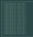
Intel's 12th Gen Core EVO "Alder Lake" processors in the LGA1700 package could introduce the company's hybrid core technology to the desktop platform. Coreboot code leaked to the web by Coelacanth's Dream sheds fascinating insights to the way Intel is segmenting these chips. The 10 nm chip will see Intel combine high-performance "Golden Cove" CPU cores with energy-efficient "Gracemont" CPU cores, and up to three tiers of the company's Gen12 Xe integrated graphics. The "Alder Lake" desktop processor has up to eight big cores, up to eight small ones, and up to three tiers of the iGPU (GT0 being disabled iGPU, GT1 being the lower tier, and GT2 being the higher tier).

Segmentation between the various brand extensions appears to be primarily determined by the number of big cores. The topmost SKU has all 8 big and 8 small cores enabled, along with GT1 (lower) tier of the iGPU (possibly to free up power headroom for those many cores). The slightly lower SKU has 8 big cores, 6 small cores, and GT1 graphics. Next up, is 8 big cores, 4 small cores, and GT1 graphics. Then 8+2+GT1, and lastly, 8+0+GT1. The next brand extension is based around 6 big cores, being led by 6+8+GT2, and progressively lower number of small cores and their various iGPU tiers. The lower brand extension is based around 4 big cores with similar segmentation of small cores, and the entry-level parts have 2 big cores, and up to 8 small cores.


View at TechPowerUp Main Site
 
Seeing this it would seem Intel has problem mixing CPU cores with iGPU in one package so iGPU tiers emerge.
 
Seeing this it would seem Intel has problem mixing CPU cores with iGPU in one package so iGPU tiers emerge.
iGPUs have always been tiered.
Intel has had GT1, GT2 and GT3e for a while now. GT1 12EU, GT2 24EU and GT3e 48EU.
Similarly, Ryzen APUs have Vega8/11 and now Vega 6/7/8 (and more in mobile).
 
I still don't see any merit in putting these products on the desktop at all.

Alder Lake is about extending battery life and endurance in connected sleep mode, simply a waste of silicon for desktops that require permanent mains power at all times.

At the low end, I think I'd rather have a 1xbig and 4xsmall over a dual-core laptop, but once you're up to 8 threads the benefit of any number of small cores seems to be nonexistent and the only purpose of the small cores is as dark silicon to act as a heatspreader for the big cores that can do the work vastly quicker and return to idle.
 
iGPUs have always been tiered.
Intel has had GT1, GT2 and GT3e for a while now. GT1 12EU, GT2 24EU and GT3e 48EU.
Similarly, Ryzen APUs have Vega8/11 and now Vega 6/7/8 (and more in mobile).
Sure but the separation for iGPUs is different. That's what I meant. You get the 8c.8small core and get lowest tier of an iGPU or no iGPU whatsoever. Previously it wasn't like that.
For example the 9900 processors got the GT2 iGPU now they don't. Maybe I didn't express myself correctly though.
 
I'm really curious to see how well this works. If all cores can run simultaneously, it could be a game changer, but if it can't run them all at the same time, it doesn't seem very useful on a desktop.
 
Running all cores simultaneously limits the big core performance to that of the small core. or 1/10, so there is no point of course.
 
I'm really curious to see how well this works. If all cores can run simultaneously, it could be a game changer, but if it can't run them all at the same time, it doesn't seem very useful on a desktop.
I don't think they can run simultaneously. The main idea with the small cores is, when full blown cores are not needed for light tasks the small cores take over to save power.
 
I still don't see any merit in putting these products on the desktop at all.

Alder Lake is about extending battery life and endurance in connected sleep mode, simply a waste of silicon for desktops that require permanent mains power at all times.

At the low end, I think I'd rather have a 1xbig and 4xsmall over a dual-core laptop, but once you're up to 8 threads the benefit of any number of small cores seems to be nonexistent and the only purpose of the small cores is as dark silicon to act as a heatspreader for the big cores that can do the work vastly quicker and return to idle.
There is one aspect that you have overlooked.
Making one core be good at low power and also at high power/performance is pretty much impossible without sacrifices.
Now, imagine Intel might wanna enlarge the big cores by a LOT. I mean, say twice the IPC compared to Skylake. That would take quite a big core to make it happen and sure, while it bring a lot of performance, in most of the tasks, that big core will be powered up for nothing.
So then they add a few smaller cores (and these smaller cores will be similar to Haswell or Zen1/Zen+, so not that bad at all) that will do all the basic stuff, web browsing, streaming, etc, etc, and then when you fire up a game or a video editing tool, all those fat cores will turn into life. You say that in desktop it doesn't matter, but people do complain about the 10900K having big power consumption. Well, a much fatter core will have a very big power consumption, so having a few smaller cores will help a lot.
It doesn't really make a ton of sense to me either, but we'll see what their motivation will be.
 
Now, imagine Intel might wanna enlarge the big cores by a LOT. I mean, say twice the IPC compared to Skylake.
If they could do that, something like this would make sense. But they absolutely cannot.

If intel could increase their IPC by even 10% (that's 10% real-world, general purpose floating point performance, not some AVX512 special instruction set that exists solely for niche uses and cheating in benchmarks) then they'd have done it on 14nm. We are at the very limits of x86 instruction execution's efficiency, with both AMD and Intel spending billions on R&D just to squeeze 5% improvements out of the architecture every 2-3 years.

Suddenly coming up with a 100% IPC improvement isn't a realistic scenario. Hell, even a 25% IPC improvement is going to raise all of the eyebrows in the room.
 
Alder Lake is about extending battery life and endurance in connected sleep mode, simply a waste of silicon for desktops that require permanent mains power at all times.

Incorrect, it's Intel's future strategy for consumer CPUs...

If intel could increase their IPC by even 10% (that's 10% real-world, general purpose floating point performance, not some AVX512 special instruction set that exists solely for niche uses and cheating in benchmarks) then they'd have done it on 14nm. We are at the very limits of x86 instruction execution's efficiency, with both AMD and Intel spending billions on R&D just to squeeze 5% improvements out of the architecture every 2-3 years.

... for the exact reasons you list above.

To be precise, Intel has figured out that big.LITTLE is the answer to their x86 scaling problem. Think about it: how many average consumers have workloads that require the full instruction set, or full clock speed, of an x86 CPU? The answer is very few, with the result that currently, x86 cores are pretty large, yet mostly underutilised.

big.LITTLE flips that paradigm so that instead of having one large, multipurpose core, you have two cores: one less powerful but also smaller, for dealing with 80% of workloads; and a standard big x86 one for the remaining 20% of high-powered workloads. Why? Because small cores are going to be just as fast as big cores for most user workloads.

Which means that instead of building an 8-big-core CPU, you build a 4-small + 4-big core CPU that performs mostly as well as the 8-core. Except it saves a massive amount of die space.

You now use that die space saving to make your big cores more powerful, and voila - your 4-small + 4-bigger core CPU can outperform your 8-big-core CPU in consumer workloads. As a bonus, it'll also be more power efficient.

big.LITTLE may not be an architecturally elegant solution, but it is a very clever solution to the problem of infinite scalability, and one that it looks like Intel has wholeheartedly embraced.
 
There is one aspect that you have overlooked.
Making one core be good at low power and also at high power/performance is pretty much impossible without sacrifices.
Now, imagine Intel might wanna enlarge the big cores by a LOT. I mean, say twice the IPC compared to Skylake. That would take quite a big core to make it happen and sure, while it bring a lot of performance, in most of the tasks, that big core will be powered up for nothing.
So then they add a few smaller cores (and these smaller cores will be similar to Haswell or Zen1/Zen+, so not that bad at all) that will do all the basic stuff, web browsing, streaming, etc, etc, and then when you fire up a game or a video editing tool, all those fat cores will turn into life. You say that in desktop it doesn't matter, but people do complain about the 10900K having big power consumption. Well, a much fatter core will have a very big power consumption, so having a few smaller cores will help a lot.
It doesn't really make a ton of sense to me either, but we'll see what their motivation will be.

Double the performance on big core is only an your dreams, is impossible.

The small ones are ATOM core not haswell/ivy/sandy brigbe on the AMD side not zen1/zen+ but more like jaguar/puma.
Small means small not a bit smaller than skylake.
 
Incorrect, it's Intel's future strategy for consumer CPUs...


... for the exact reasons you list above.

To be precise, Intel has figured out that big.LITTLE is the answer to their x86 scaling problem. Think about it: how many average consumers have workloads that require the full instruction set, or full clock speed, of an x86 CPU? The answer is very few, with the result that currently, x86 cores are pretty large, yet mostly underutilised.

big.LITTLE flips that paradigm so that instead of having one large, multipurpose core, you have two cores: one less powerful but also smaller, for dealing with 80% of workloads; and a standard big x86 one for the remaining 20% of high-powered workloads. Why? Because small cores are going to be just as fast as big cores for most user workloads.

Which means that instead of building an 8-big-core CPU, you build a 4-small + 4-big core CPU that performs mostly as well as the 8-core. Except it saves a massive amount of die space.

You now use that die space saving to make your big cores more powerful, and voila - your 4-small + 4-bigger core CPU can outperform your 8-big-core CPU in consumer workloads. As a bonus, it'll also be more power efficient.

big.LITTLE may not be an architecturally elegant solution, but it is a very clever solution to the problem of infinite scalability, and one that it looks like Intel has wholeheartedly embraced.

They still have work to do though because it doesnt look like the big cores are actually faster, just yet.
 
Incorrect, it's Intel's future strategy for consumer CPUs...


... for the exact reasons you list above.

To be precise, Intel has figured out that big.LITTLE is the answer to their x86 scaling problem. Think about it: how many average consumers have workloads that require the full instruction set, or full clock speed, of an x86 CPU? The answer is very few, with the result that currently, x86 cores are pretty large, yet mostly underutilised.

big.LITTLE flips that paradigm so that instead of having one large, multipurpose core, you have two cores: one less powerful but also smaller, for dealing with 80% of workloads; and a standard big x86 one for the remaining 20% of high-powered workloads. Why? Because small cores are going to be just as fast as big cores for most user workloads.

Which means that instead of building an 8-big-core CPU, you build a 4-small + 4-big core CPU that performs mostly as well as the 8-core. Except it saves a massive amount of die space.

You now use that die space saving to make your big cores more powerful, and voila - your 4-small + 4-bigger core CPU can outperform your 8-big-core CPU in consumer workloads. As a bonus, it'll also be more power efficient.

big.LITTLE may not be an architecturally elegant solution, but it is a very clever solution to the problem of infinite scalability, and one that it looks like Intel has wholeheartedly embraced.
Isn't one of the biggest factors in making the Atom cores smaller just a stripped down instruction set? You're advocating that consumer workloads don't need all the added guff like x87, IA-32, MMX, SSE, SSE2, SSE3, SSSE3, SSE4, SSE4.2, SSE5, AES-NI, CLMUL, RDRAND, SHA, MPX, SGX, XOP, F16C, ADX, BMI, FMA, AVX, AVX2, AVX512, VT-x, TSX, ASF....

Yeah, I'm all in favour of removing most of those things from consumer processors. But I don't want crippled pipelines, inefficient cache splits, poor branch prediction and resource conflicts. Linus Torvalds was on point when he slammed intel last month for adding useless, edge-case BS to their chips instead of just offering more general-purpose cores that work well for anything. Give me big, unified caches, great branch predictors, strong FPU performance and more cores. By all means, focus on a couple for max boost frequency - in other words make sure they have the cleanest voltage and the shortest number of domain hops to supporting logic, but more than that - just give us more cores; They can be parked when idle if power consumption is the problem, exactly how the BIG cores of Alder Lake will be parked when the little cores are handling everything.

Outside of SSE (probably SSE3) many of Intel's x86 extensions are just wasted silicon on a consumer processor. I freely admit that I don't even know what all of those acronyms are in that list I copied from the Wiki on x86 but that surely means they're simply not that common and therefore niche enough to be axed.
 
Last edited:
I tend to think that if Intel is smart they'll remove the older weaker, and more redundant instruction sets on the stronger big cores and place them exclusively on the weaker atom cores.
 
It's interesting that as Apple leaves Intel to go with big.LITTLE with its Apple Silicon chips, Intel is shifting to big.LITTLE as well. People seem pretty intrigued by the possibilities of Apple Silicon, or at least no one seems to be writing it off as a lost cause already just because it's going to be big.LITTLE. Obviously Apple's execution has been a lot better than Intel's in the last few years so it's fair Apple gets the benefit of the doubt while Intel very much needs to prove it can pull another rabbit out of its hat like Core. I guess we will see if Intel can execute.
 
There is one aspect that you have overlooked.
Making one core be good at low power and also at high power/performance is pretty much impossible without sacrifices.
Now, imagine Intel might wanna enlarge the big cores by a LOT. I mean, say twice the IPC compared to Skylake. That would take quite a big core to make it happen and sure, while it bring a lot of performance, in most of the tasks, that big core will be powered up for nothing.
So then they add a few smaller cores (and these smaller cores will be similar to Haswell or Zen1/Zen+, so not that bad at all) that will do all the basic stuff, web browsing, streaming, etc, etc, and then when you fire up a game or a video editing tool, all those fat cores will turn into life. You say that in desktop it doesn't matter, but people do complain about the 10900K having big power consumption. Well, a much fatter core will have a very big power consumption, so having a few smaller cores will help a lot.
It doesn't really make a ton of sense to me either, but we'll see what their motivation will be.

I have a tiny bit of interest in this for VM purposes. If it's cheaper than just 12-16 big cores from Intel or AMD. If the security problems can be largely resolved for the uarch. Since I can have all of the helper threads (I/O and host) sit on the small cores while the VMs feast on the large cores. Again, if it's not cheaper than 12-16 large cores, then no way will this be worth it, unless if it's bringing significant platform features (32+ PCIe 4.0 lanes, etc).
 
I really don't see much point in this. At least not for my use. I will prefer any time 16 powerful cores.

I can see the benefits for laptops, phones, tablets and other battery using devices. There this idea can come in handy. But desktop use, not so much. You are plugged in all the time and don't have to worry about battery life. If the pc is on 24 hours a day and dosent do much most of the time. I can see some idea of low power cores being only active. Else desktop I can't see so much benefit of low power cores, specially if these cores are based on atom cores and boy the atom quad core i had last year whas a slow piece of useless lump of plastic. CB R15 score whas single core 25 and multi 99. My old i7 980x oc to 4.4 ghz scores 133 in single cores so one core of my 10 years old cpu overclock is more powerful than and entire atom quad-core cpu. I shall never own a atom powered pc ever again. Utter useless cpu.
 
Unless they fix the unmatched cure features we saw on Lakefield, then this is DOA,.

They had to disable AVX (all versions) AND hyperthreading to make this work seamlessly, so unless they want us to disable these pointless cores, they better got cracking and add these features to Gracemont.
 
If they could do that, something like this would make sense. But they absolutely cannot.

If intel could increase their IPC by even 10% (that's 10% real-world, general purpose floating point performance, not some AVX512 special instruction set that exists solely for niche uses and cheating in benchmarks) then they'd have done it on 14nm. We are at the very limits of x86 instruction execution's efficiency, with both AMD and Intel spending billions on R&D just to squeeze 5% improvements out of the architecture every 2-3 years.

Suddenly coming up with a 100% IPC improvement isn't a realistic scenario. Hell, even a 25% IPC improvement is going to raise all of the eyebrows in the room.
First, they cannot do big IPC increase on 14nm since it would take a lot of die space.
Second, they already have 18% IPC boost with Ice Lake and will add another 5-10% over that with the new Tigerlake core in September.
Maybe you are not aware of that, but 1065G7 tested at the same frequency with a 3900x has 5-10% IPC advantage.
If you take a look over the presentation that Jim K has done while he was at Intel, he clearly stated that his focus is to create a core that is a magnitude bigger and more complex than what Skylake is. Also, there are lots of rumours circulating about Golden Cove, which is used in Alder Lake that it has 50% better IPC than Skylake. I don't think that is impossible and not even unlikely.
I believe many people are making today a very big mistake when judging Intel. They extrapolate their fabrication issues with IP/design/architectural issues. Intel doesn't have any problem on the architectural side of things. Give them a good process and they can make either a slim core with high efficiency or a phat core, no problem. I would argue that at Intel there is a lot more talent compared to AMD, but their management issues are very deep and engineers are not really allowed to focus on engineering excellence because of a more business focused approach.
I don't think you imagine that all the design teams that Intel has have stayed idle during 2015-2020. They have created new cores, new uArchs, new IPs, but they just couldn't fabricate them with reasonable costs.

Double the performance on big core is only an your dreams, is impossible.

The small ones are ATOM core not haswell/ivy/sandy brigbe on the AMD side not zen1/zen+ but more like jaguar/puma.
Small means small not a bit smaller than skylake.
Technically 100% IPC is doable. If you double the execution units and make the core to be able to feed those units I don't see why you couldn't have a big IPC increase. Actually, Skylake currently has a lot more execution power unused that could mean higher IPC if they would improve the front end. Also, adding caches helps a lot with the IPC if you don't use your execution units fully, so that is what Apple did, what AMD did with Zen 2 and what Intel will do with Tigerlake. Everything at some point is deemed impossible and then someone comes and makes it possible. If you're not a dreamer, better get another job.

In regards to small cores, what is exactly your point? Tremont has Ivy bridge level of IPC. Zen 1 has Ivy bridge - haswell level of IPC.
If Tremont has IPC comparable to Ivy, this doesn't mean the core is as phat as Skylake...
You can search for die shots, but 4 tremont cores are just a bit more than 1 sunny cove core in die size, so I would estimate 1 tremont core to be 1 third of a skylake core. Given it has ivy bridge level of IPC, that is very impressive.
 
Last edited:
Technically 100% IPC is doable. If you double the execution units and make the core to be able to feed those units I don't see why you couldn't have a big IPC increase. Actually, Skylake currently has a lot more execution power unused that could mean higher IPC if they would improve the front end. Also, adding caches helps a lot with the IPC if you don't use your execution units fully, so that is what Apple did, what AMD did with Zen 2 and what Intel will do with Tigerlake. Everything at some point is deemed impossible and then someone comes and makes it possible. If you're not a dreamer, better get another job.
I think that would not result in that large of an IPC increase in any real application. Going wider helps with something that is compute heavy and/or parallelizable, less with something like desktop/browser usage or games.

Although people from Intel have hinted or said there is unused execution power, I would suspect Zen has more. If you look at Skylake execution units vs Zen ones AMD has taken a cool approach of relatively simple units. Intel has a couple big, powerful multipurpose units against AMD's more purpose-focused units that Zen has more of. This is probably why Zen's SMT works measurably better than Skylake's HT - it has more (or more easily workable) set of execution units.

I bet that Intel's reason for having these complex units - other than historical/legacy - is that they are very optimal in transistor cost.
 
Intel doesn't have any problem on the architectural side of things. Give them a good process and they can make either a slim core with high efficiency or a phat core, no problem. I would argue that at Intel there is a lot more talent compared to AMD

I simply don't agree with that at all.

Even if you ignore the issues intel is having with 10nm and now 7nm, that doesn't change the fact that Intel's architecture is old and riddled with security problems. That's not a process issue, that's an architecture issue. A lot of intel's historic IPC has been proven to be shortcuts that sidestep security. Cheating, if you want to call it that. Once all the relevant security patches are in place, Intel CPUs have significantly lower IPC than Zen2 right now, and it's STILL riddled with security issues that are being discovered faster than Intel can patch them.

As for the quality of that architecture, Zen2 outperforms Intel's current architecture in terms of IPC. The only reason Intel has a perceived advantage is that when clocked to 5.3GHz, intel is quicker than AMD at 4.7GHz. When you take a clock-locked 4GHz Intel and a 4GHz Zen2, the AMD architecture will win in a majority of applications. Gaming is a notable exception and I believe a big part of that difference is the added latency between cores and the memory controller by having them in physically isolated packages over a seperately-clocked bus (Infinity fabric).

AMD have overtaken Intel in architecture, and they've done it on 1/10th the budget of Intel's R&D department. All that talent Intel may have is pointless and completely academic if it's not being used.
AMD are also on track for a >10% IPC gain with Zen3 and that alone should be enough to prove to anyone that AMD's architecture is vastly superior to Intel's dated, insecure ****lake architecture - there simply won't be enough clockspeed advantage for Intel to make up the difference....

Competition is good. I'll praise Intel when they actually make a clean, new architecture that can provide higher IPC than AMD. As it stands, their architecture is old, stagnant and insecure. Aside from a few reasonably decent increments (like Skylake and Coffee Lake) it's still basically just a tweaked Sandy Bridge as the underlying architecture - and Sandy Bridge is only a few months away from its 10th anniversary now.

To be in such a sorry state with the talent and finances Intel have after a decade of the same architecture is downright inexcusable.
 
that doesn't change the fact that Intel's architecture is old and riddled with security problems.
Ice Lake? Tiger Lake? They are not that old.
When you take a clock-locked 4GHz Intel and a 4GHz Zen2, the AMD architecture will win in a majority of applications.
Intel? This is correct about Skylake and not correct about Ice Lake.
AMD have overtaken Intel in architecture, and they've done it on 1/10th the budget of Intel's R&D department.
Do you have a breakdown on Intel's R&D costs per department? This would be an awesome read but I have not been able to find even a good analysis on that. Intel does a lot more than AMD with its R&D budget, foundry alone is responsible for several billion dollars yearly, and this is using a conservative estimate.
 
Ice Lake? Tiger Lake? They are not that old.
Intel? This is correct about Skylake and not correct about Ice Lake.
Ice Lake is an improvement, I believe. I haven't read a deep dive on Sunny Cove yet but hopefully it's a 'clean' start and secure, not just an incremental evolution of SkyLake.

In terms of execution, Ice Lake architecture should have been transitioned to 14nm as soon as Intel realised that 10nm wouldn't scale beyond small die, low-power mobile parts. Again, that's a process node problem and nothing to do with the architecture.

IMO Intel should have back-ported Ice Lake/Sunny Cove to 14+++ two years ago so that it was on the market last year to compete with Zen2. Instead they've been in this death-spiral of squeezing *lake to death despite all the scalability and security issues that plague it's core DNA.
 
Instead they've been in this death-spiral of squeezing *lake to death despite all the scalability and security issues that plague it's core DNA.

You're going to have to substantiate your claim that the Skylake uarch, and its derivatives, have ingrained scalability and security issues. Sunny Cove is a derivative of Skylake, which is a derivative of Sandy Bridge, and the IPC increase from the original SNB parts to those of today are massive. Not to mention that SKL => SNC is supposedly an 18% IPC improvement again... a uarch that can be competitive for nearly a decade sounds pretty scalable to me.

SNC being first detailed in 2018 is irrelevant, do you really think Intel's architecture teams have been sitting on their thumbs for 2 whole years? You don't seem to understand that while arch has somewhat of a dependence on fab, there's nothing stopping arch from pursuing all sorts of interesting concepts while they're waiting for fab to get its shit together. Hence Lakefield.
 
Back
Top