- Joined
- Oct 9, 2007
- Messages
- 47,880 (7.38/day)
- Location
- Dublin, Ireland
| System Name | RBMK-1000 |
|---|---|
| Processor | AMD Ryzen 7 5700G |
| Motherboard | Gigabyte B550 AORUS Elite V2 |
| Cooling | DeepCool Gammax L240 V2 |
| Memory | 2x 16GB DDR4-3200 |
| Video Card(s) | Galax RTX 4070 Ti EX |
| Storage | Samsung 990 1TB |
| Display(s) | BenQ 1440p 60 Hz 27-inch |
| Case | Corsair Carbide 100R |
| Audio Device(s) | ASUS SupremeFX S1220A |
| Power Supply | Cooler Master MWE Gold 650W |
| Mouse | ASUS ROG Strix Impact |
| Keyboard | Gamdias Hermes E2 |
| Software | Windows 11 Pro |
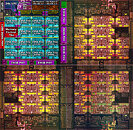
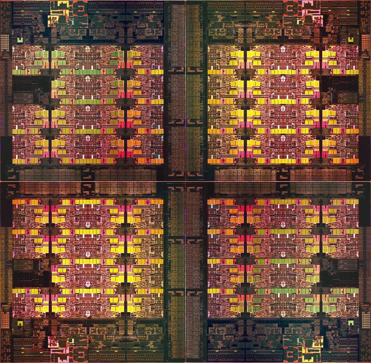
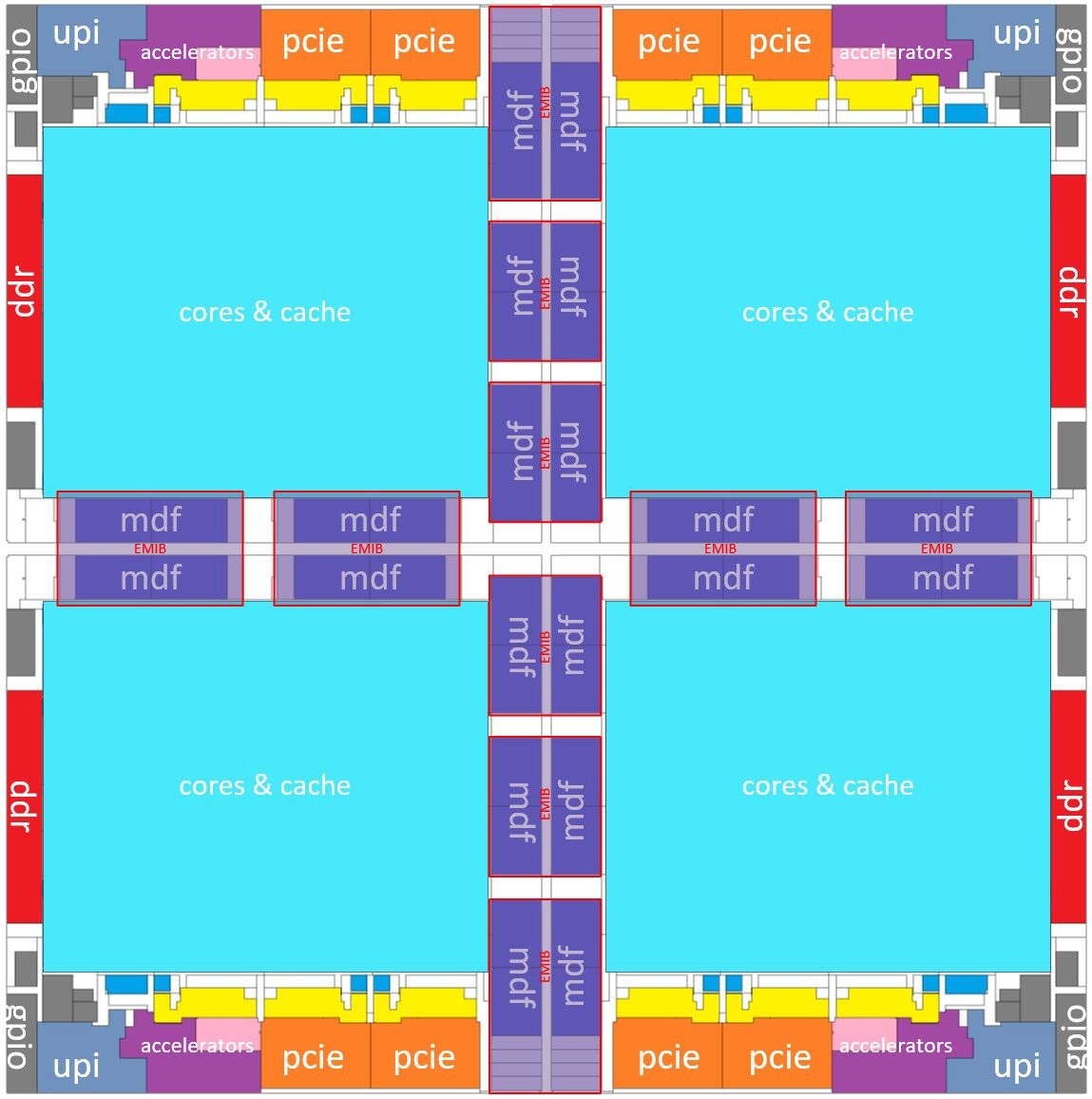
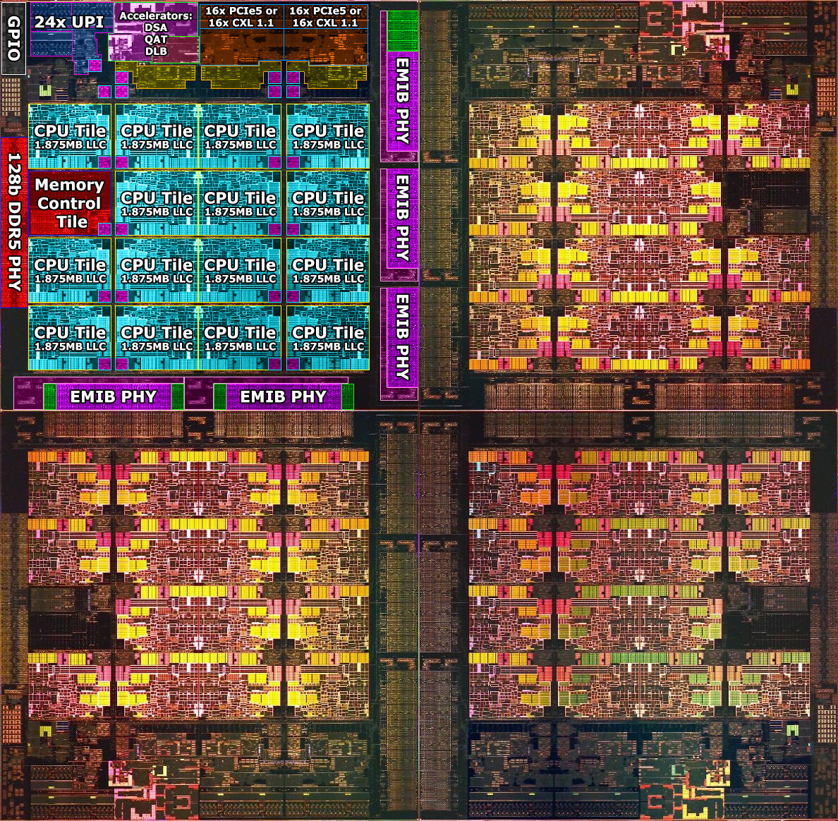
Intel Xeon Scalable "Sapphire Rapids" is an upcoming enterprise processor with a CPU core count of up to 60. This core-count is achieved using four dies inter-connected using EMIB. Locuza, who leads social media with logic die annotation, posted one for "Sapphire Rapids," based on a high-resolution die-shot revealed by Intel in its ISSCC 2022 presentation.
Each of the four dies in "Sapphire Rapids" is a fully-fledged multi-core processor in its own right, complete with CPU cores, integrated northbridge, memory and PCIe interfaces, and other platform I/O. What brings four of these together is the use of five EMIB bridges per die. This allows CPU cores of a die to transparantly access the I/O and memory controlled any of the other dies transparently. Logically, "Sapphire Rapids" isn't unlike AMD "Naples," which uses IFOP (Infinity Fabric over package) to inter-connect four 8-core "Zeppelin" dies, but the effort here appears to be to minimize the latency arising from an on-package interconnect, toward a high-bandwidth, low-latency one that uses silicon bridges with high-density microscopic wiring between them (akin to an interposer).
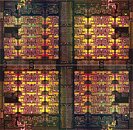

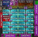
Within each die, the floor-plan is similar to several past generations of Intel enterprise processors. Intel uses the Mesh interconnect, and lays the various IP blocks across a grid, interconnecting them in a mesh of ring-buses. Mesh is a middle-ground between a ring-bus and full point-to-point interconnectivity. Each individual component in the Mesh is called a "tile." The die contains fifteen "Golden Cove" CPU cores, each with 2 MB of dedicated L2 cache, and a 1.875 MB slice of last-level cache that contributes toward 28,800 KB (28.125 MB) of L3 cache that's shared among all 60 cores of the processor. The total L3 cache for the package is 112.5 MB.
Each die also features a memory-controller tile, with a 128-bit (160-bit including ECC) DDR5 PHY. This interface controls two DDR5 channels, which amounts to four 40-bit sub-channels. The package in total supports eight DDR5 channels (16 sub-channels). The PCIe/CXL interface for "Sapphire Rapids" is massive. Each die features a PCI-Express Gen 5 + CXL 1.1 root-complex with 32 lanes, working out to 128 PCI-Express Gen 5 or CXL 1.1 lanes.
The Accelerator tile packs Intel Data-Streaming Accelerator (DSA), QuickAssist Technology (QAT); and DLBoost 2.0, a hardware component that accelerates deep-learning neural net building and training.
The final kind of tile packs 24x UPI links that work as an inter-socket interconnect. Each of the four dies has this, making "Sapphire Rapids" technically capable of 8P.
View at TechPowerUp Main Site | Source
Each of the four dies in "Sapphire Rapids" is a fully-fledged multi-core processor in its own right, complete with CPU cores, integrated northbridge, memory and PCIe interfaces, and other platform I/O. What brings four of these together is the use of five EMIB bridges per die. This allows CPU cores of a die to transparantly access the I/O and memory controlled any of the other dies transparently. Logically, "Sapphire Rapids" isn't unlike AMD "Naples," which uses IFOP (Infinity Fabric over package) to inter-connect four 8-core "Zeppelin" dies, but the effort here appears to be to minimize the latency arising from an on-package interconnect, toward a high-bandwidth, low-latency one that uses silicon bridges with high-density microscopic wiring between them (akin to an interposer).

Within each die, the floor-plan is similar to several past generations of Intel enterprise processors. Intel uses the Mesh interconnect, and lays the various IP blocks across a grid, interconnecting them in a mesh of ring-buses. Mesh is a middle-ground between a ring-bus and full point-to-point interconnectivity. Each individual component in the Mesh is called a "tile." The die contains fifteen "Golden Cove" CPU cores, each with 2 MB of dedicated L2 cache, and a 1.875 MB slice of last-level cache that contributes toward 28,800 KB (28.125 MB) of L3 cache that's shared among all 60 cores of the processor. The total L3 cache for the package is 112.5 MB.
Each die also features a memory-controller tile, with a 128-bit (160-bit including ECC) DDR5 PHY. This interface controls two DDR5 channels, which amounts to four 40-bit sub-channels. The package in total supports eight DDR5 channels (16 sub-channels). The PCIe/CXL interface for "Sapphire Rapids" is massive. Each die features a PCI-Express Gen 5 + CXL 1.1 root-complex with 32 lanes, working out to 128 PCI-Express Gen 5 or CXL 1.1 lanes.
The Accelerator tile packs Intel Data-Streaming Accelerator (DSA), QuickAssist Technology (QAT); and DLBoost 2.0, a hardware component that accelerates deep-learning neural net building and training.
The final kind of tile packs 24x UPI links that work as an inter-socket interconnect. Each of the four dies has this, making "Sapphire Rapids" technically capable of 8P.
View at TechPowerUp Main Site | Source


