- Joined
- Oct 9, 2007
- Messages
- 47,895 (7.38/day)
- Location
- Dublin, Ireland
| System Name | RBMK-1000 |
|---|---|
| Processor | AMD Ryzen 7 5700G |
| Motherboard | Gigabyte B550 AORUS Elite V2 |
| Cooling | DeepCool Gammax L240 V2 |
| Memory | 2x 16GB DDR4-3200 |
| Video Card(s) | Galax RTX 4070 Ti EX |
| Storage | Samsung 990 1TB |
| Display(s) | BenQ 1440p 60 Hz 27-inch |
| Case | Corsair Carbide 100R |
| Audio Device(s) | ASUS SupremeFX S1220A |
| Power Supply | Cooler Master MWE Gold 650W |
| Mouse | ASUS ROG Strix Impact |
| Keyboard | Gamdias Hermes E2 |
| Software | Windows 11 Pro |
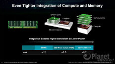
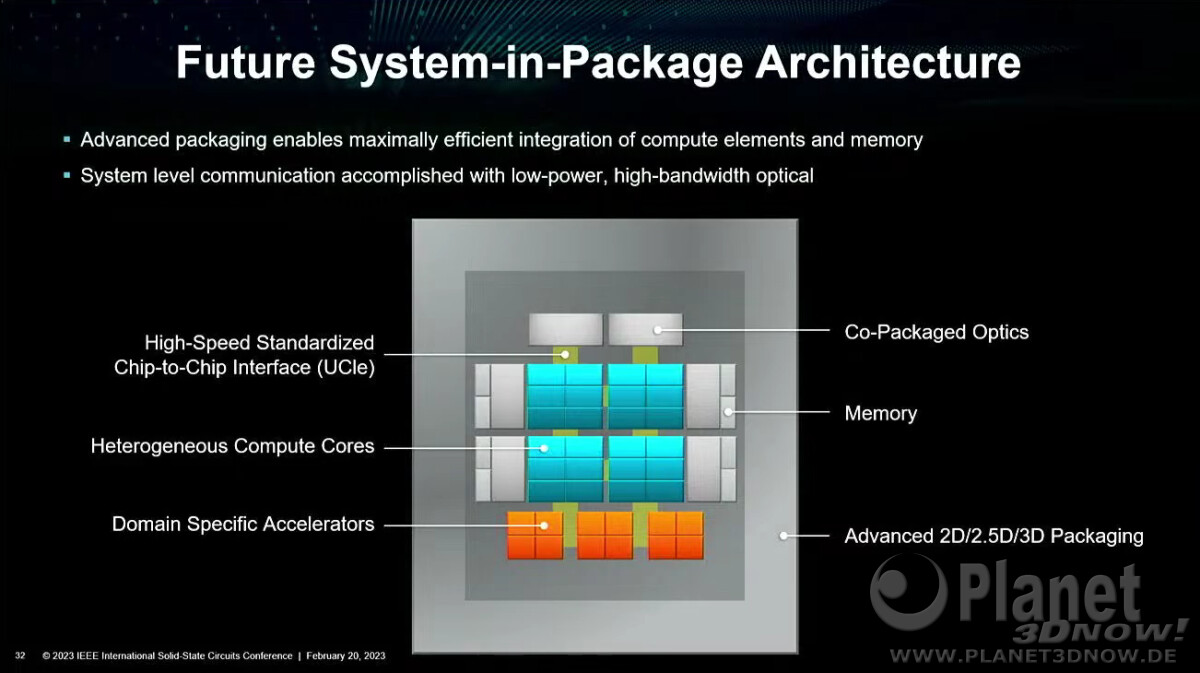
AMD in its ISSCC 2023 presentation detailed how it has advanced data-center energy-efficiency and managed to keep up with Moore's Law, even as semiconductor foundry node advances have tapered. Perhaps its most striking prediction for server processors and HPC accelerators is multi-layer stacked DRAM. The company has, for some time now, made logic products, such as GPUs, with stacked HBM. These have been multi-chip modules (MCMs), in which the logic die and HBM stacks sit on top of a silicon interposer. While this conserves PCB real-estate compared to discrete memory chips/modules; it is inefficient on the substrate, and the interposer is essentially a silicon die that has microscopic wiring between the chips stacked on top of it.
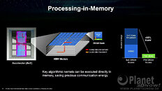
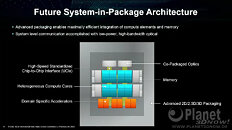
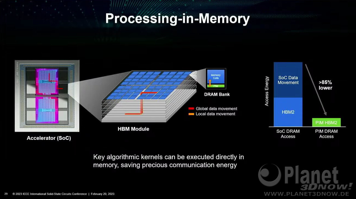
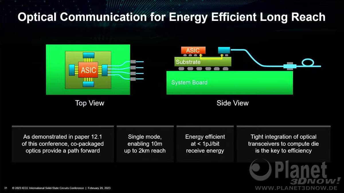
AMD envisions that the high-density server processor of the near-future will have many layers of DRAM stacked on top of logic chips. Such a method of stacking conserves both PCB and substrate real-estate, allowing chip-designers to cram even more cores and memory per socket. The company also sees a greater role of in-memory compute, where trivial simple compute and data-movement functions can be executed directly on the memory, saving round-trips to the processor. Lastly, the company talked about the possibility of an on-package optical PHY, which would simplify network infrastructure.

View at TechPowerUp Main Site | Source
AMD envisions that the high-density server processor of the near-future will have many layers of DRAM stacked on top of logic chips. Such a method of stacking conserves both PCB and substrate real-estate, allowing chip-designers to cram even more cores and memory per socket. The company also sees a greater role of in-memory compute, where trivial simple compute and data-movement functions can be executed directly on the memory, saving round-trips to the processor. Lastly, the company talked about the possibility of an on-package optical PHY, which would simplify network infrastructure.
View at TechPowerUp Main Site | Source


")


