Tuesday, February 21st 2023

AMD Envisions Stacked DRAM on top of Compute Chiplets in the Near Future

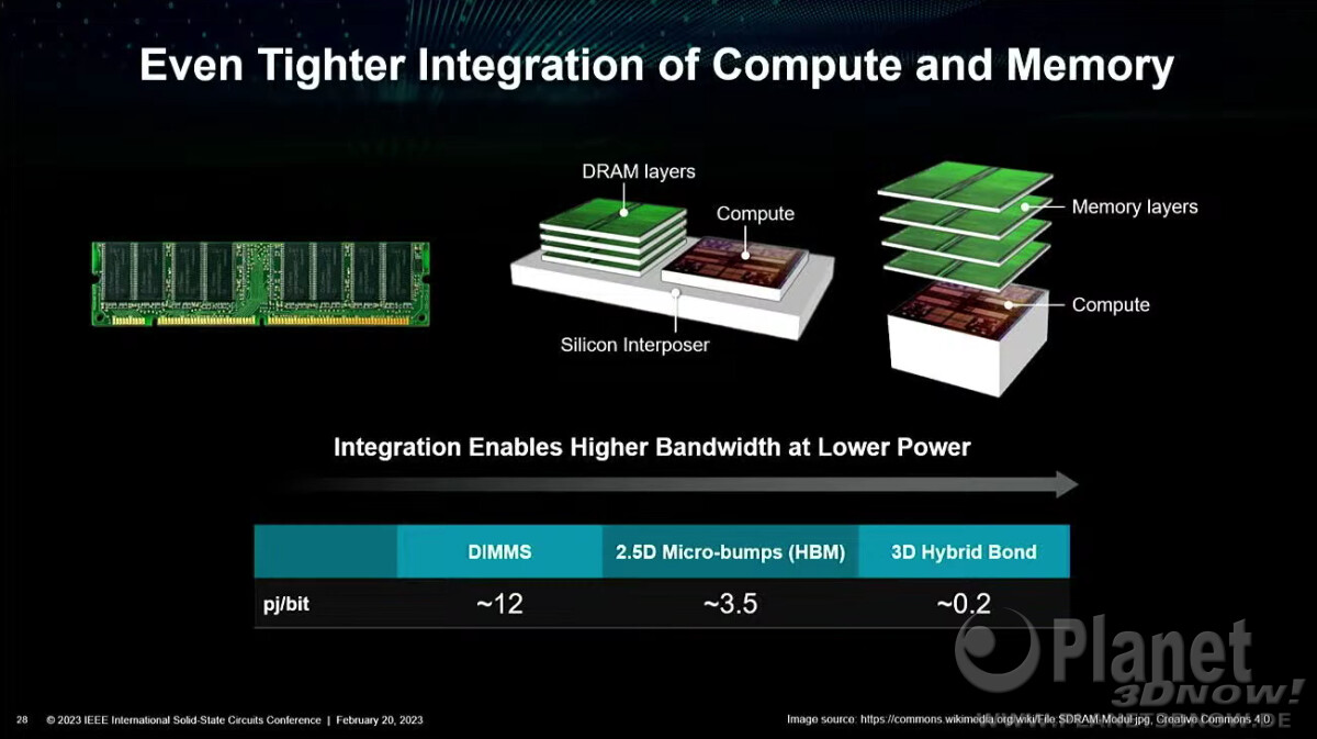
AMD in its ISSCC 2023 presentation detailed how it has advanced data-center energy-efficiency and managed to keep up with Moore's Law, even as semiconductor foundry node advances have tapered. Perhaps its most striking prediction for server processors and HPC accelerators is multi-layer stacked DRAM. The company has, for some time now, made logic products, such as GPUs, with stacked HBM. These have been multi-chip modules (MCMs), in which the logic die and HBM stacks sit on top of a silicon interposer. While this conserves PCB real-estate compared to discrete memory chips/modules; it is inefficient on the substrate, and the interposer is essentially a silicon die that has microscopic wiring between the chips stacked on top of it.

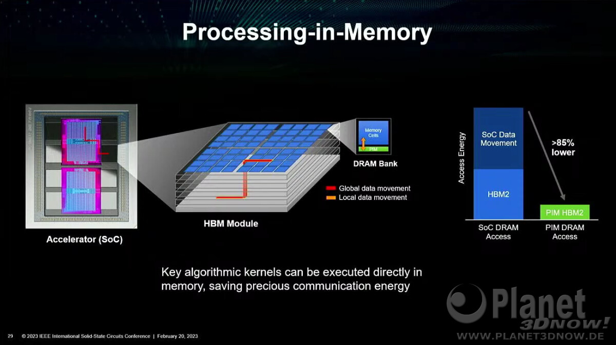
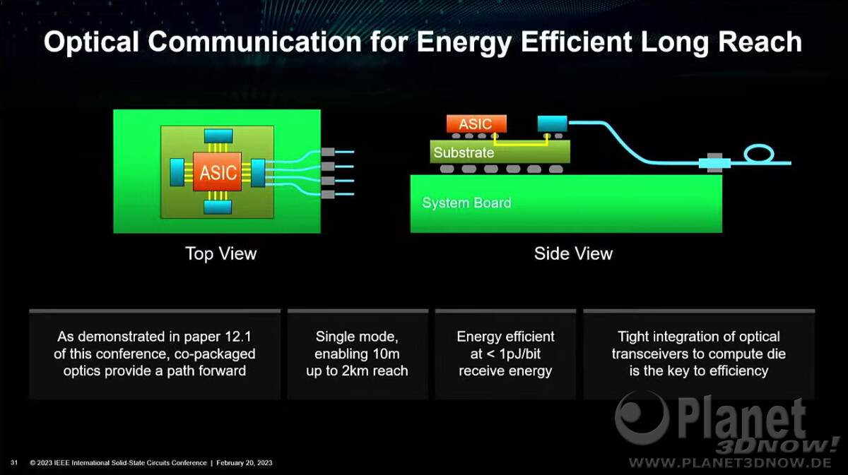
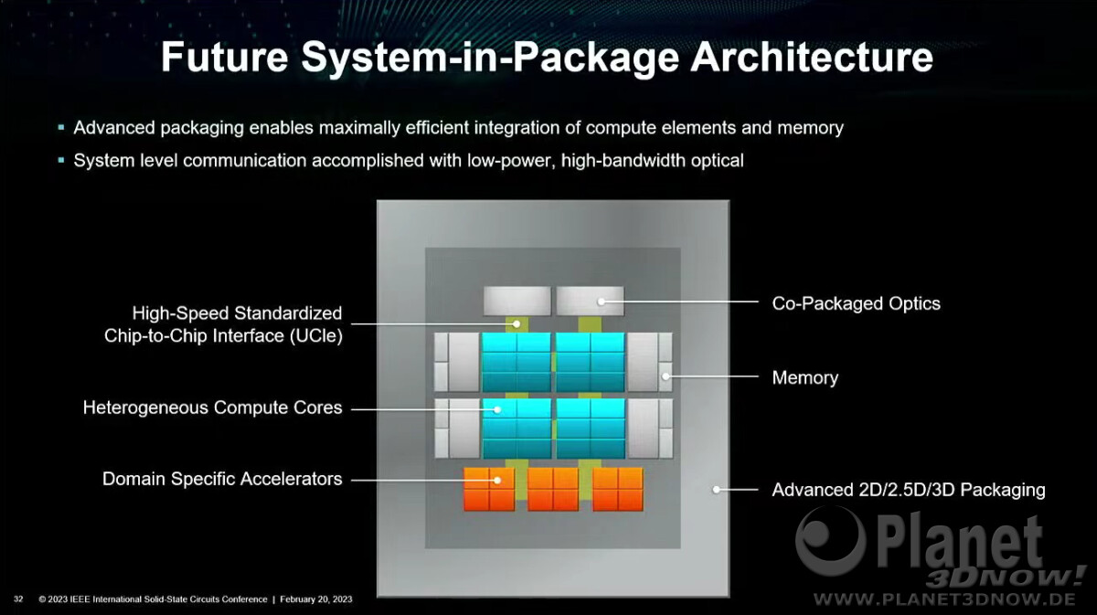
AMD envisions that the high-density server processor of the near-future will have many layers of DRAM stacked on top of logic chips. Such a method of stacking conserves both PCB and substrate real-estate, allowing chip-designers to cram even more cores and memory per socket. The company also sees a greater role of in-memory compute, where trivial simple compute and data-movement functions can be executed directly on the memory, saving round-trips to the processor. Lastly, the company talked about the possibility of an on-package optical PHY, which would simplify network infrastructure.
Source: Planet3DNow.de
Add your own comment

25 Comments on AMD Envisions Stacked DRAM on top of Compute Chiplets in the Near Future

#1
nguyen
Should be great for mobile gaming, as for desktop, not so much...
Posted on Reply
#2
Chaitanya
Given how well 3DV cache works having some DRAM(additional tier of memory) close to cpu die will be greatly helpful for whole range of applications.
Posted on Reply
#3
Dirt Chip
Any thoughts on how to effectively cool this stacked tower?
Or this only aimed at low frequency, high core count server CPU`s?

Anyway, nice innovation.
Posted on Reply
#4
Tomorrow
I see the point for mobile where space and energy savings are important or servers where compute per area matters but on desktop it's a tough ask. Current iterations of L3 cache sit on top of existing L3 on the chipset. Even so it compromises the chipset boost clock speeds due to voltage limitations and has issues with cooling.

So if AMD plans to utilize this in the future they and TSMC have to first solve the cooling and compromised clocks issue. 7800X3D loses 400-700Mhz of potential boost due to these issues. That's a significant chunk of clock speed.

The other issue is release timing. Currently it takes half a year before desktop gets X3D models. I hope in the future these will be the default on day 1 launch of a new architecture.
But stacking clearly is the future. Sockets are already enormous. Desktop sockets already approach 2000 pins and server sockets exceed 6000.
Posted on Reply
#6
delshay
Now they talking my cup of tea. Big fan of HBM Memory, this is why I stuck with my R9/Vega Nano cards. HBM-PIM was talked about some time ago by Samsung.

Very short read here High Bandwidth Memory - Wikipedia
Posted on Reply
#8
Minus Infinity
HBM3 prices have just been increased enormously. Let's see what customers think of the new pricing down the track.
Posted on Reply
#9
InVasMani
The optical part has me fascinated reminds me of some of this discussion I had raised about them and me trying to just brainstorm where and how might these be applied that could work and make sense and provide innovation at the same time.

www.techpowerup.com/forums/threads/nvidia-is-preparing-co-packaged-photonics-for-nvlink.276139/#post-4418550

Another thing related to optic I had mentioned was this.

"I could see a optical path potentially interconnecting them all quickly as well."

That was in regard to FPGA/CPU/GPU chiplets as well as 3Dstacking.

I spoke some about combining DIMM's with chiplets and felt it could be a good if for no other reason than for compression/decompression from those. This is neat though combining TSV and a chiplet and stacking DRAM directly on top of it. Perhaps some optical interconnects in place of TSV could work too. I think that would add another layer of complications though if you had the optical connection on substrate and then used a optical connect in place of TSV you could shave off some latency I think. I don't know maybe that's a bit of what they've already envisioned here though.

Eventually they could maybe have a I/O die in the center and 8 surrounding chiplets on a substrate and below that another substrate connected to it optically with 3D stacked cache. The way it could connect with the substrate above is each chiplet along the edge around the I/O could connect to a optical connection to the 3D stacked cache below. In fact you could even cool it a bit as well because the cache itself can be inverted and cooled on that side regardless of the optical easily enough. The only barrier I see is the cost of optics and how well it can be shrunk down in size at the same time for functionality as a interconnect.
Posted on Reply
#10
LiviuTM
Guys, don't get too excited yet. These technologies will surely be quite expensive in the beginning, slim chances to see them soon in consumer products.
Posted on Reply
#11
ymdhis
I have been envisioning this ever since the first HBM GPU came out. Putting 16/32GB of HBM/2/3 next to a CPU would allow for memory speeds in excess of any DDR4/5 stick, and it would save a tremendous amount of space on the motherboard. Put a decent iGPU in such a chip and it would all but eliminate the mid-range gpu market. And I'm sure that greedy cpu makers like Intel would cream their pants at the possibility of offering every cpu in 2-5 different SKUs based on inbuilt memory amount.
With chiplets it could even be more feasible; one cpu core, one gpu core, one memory controller, and one or multiple HBM stacks. It would be perfect for both consoles and SFF builds.
Posted on Reply
#12
Wirko
Minus InfinityHBM3 prices have just been increased enormously. Let's see what customers think of the new pricing down the track.
The same packaging tech is also usable for integrating DDR or LPDDR.

HBM isn't universally better, it requires more exotic dense interconnects and giant memory controllers.
Posted on Reply
#13
delshay
WirkoThe same packaging tech is also usable for integrating DDR or LPDDR.

HBM isn't universally better, it requires more exotic dense interconnects and giant memory controllers.
Are you sure? I do believe HBM controller is smaller than GDDR(x). ...it's certainly more efficient & requires less power.
Posted on Reply
#14
Xajel
I guessed this long time ago to be the future of all PCs.

But, prosumer & consumer products will still need an upgradable RAM of some sort.

I mean the stacked DRAM is there for sure, but the CPU/SoC should still keep the 128/160bit IMC there for expandability. The thing will be tiered Memory Hierarchy will prioritize processes for the Stacked DRAM and/or regular RAM depending on Power/Bandwidth/Latency requirements.

Depending on how hard and costly is the stacked DRAM, AMD might have one or two options, and big OEMs might request some custom orders.
Posted on Reply
#15
Denver
This is the most exciting thing I've seen in a long time. This would certainly be a huge step forward for the server market.
Posted on Reply
#16
Panther_Seraphin
HBM as a Pseudo L4 cache would be a big benefit to a lot of things as X3D has proven that there is a lot of software/games/databases that would take advantage of the wider/faster transfer speeds of HBM vs traditional DRAM.

However there would nearly always be a need for DRAM connectivity as datasets are growing quicker in most areas than what is feesible with direct memory. (Currently capable of 6TB of memory per socket in the server space)

Also you are adding more power requirements to the CPU die (~30 watts) just for the HBM and would need a radically different I/O die to accomodate its integration. So you start running into packaging issues as the size of some of the server CPUs are getting into the realms of ridiculousness. (Consumer CPUs are 4x4Cm2 where as newest AMD Genoa is already pushing 7.5x7.5Cm2)
Posted on Reply
#17
Punkenjoy
nguyenShould be great for mobile gaming, as for desktop, not so much...
That depend, it would suck if they remove the ability to add more memory via DIMM slots on the motherboard. Else it might not.
Panther_SeraphinHBM as a Pseudo L4 cache would be a big benefit to a lot of things as X3D has proven that there is a lot of software/games/databases that would take advantage of the wider/faster transfer speeds of HBM vs traditional DRAM.

However there would nearly always be a need for DRAM connectivity as datasets are growing quicker in most areas than what is feesible with direct memory. (Currently capable of 6TB of memory per socket in the server space)

Also you are adding more power requirements to the CPU die (~30 watts) just for the HBM and would need a radically different I/O die to accommodate its integration. So you start running into packaging issues as the size of some of the server CPUs are getting into the realms of ridiculousness. (Consumer CPUs are 4x4Cm2 where as newest AMD Genoa is already pushing 7.5x7.5Cm2)
That really depend on how much memory they add on top of the die, if they add more than few GB, a cache would be hard to maintain and it's possible it would be better to just use that memory as standard memory (and bypass all the cache lookup thing). We can do that with NUMA. Memory tiering would be something new on desktop but not on server and mainframe.

It could require some time for Windows to adapt but imagine you have 16 GB on top of your APU and then 32 GB or more of DDR5 DIMM. You play a game and the OS put the most used data into the on die memory and all the extra stuff get moved to the slower DIMM.

If you use less than 16 GB of ram, the DIMM memory could be powered down.
Posted on Reply
#18
ymdhis
Re-reading the article, they are talking not about using HBM, but by stacking HBM *on top* of the cpu/gpu. Basically imagine the 3d stacking on the 5800X3D, but with 8GB 1024bit modules.

That makes a lot more sense than just adding HBM on an interposer, and may be simpler to manufacture (since they don't need the interposer itself). It would remove one of the big problems of using HBM and make it a lot more viable.
Posted on Reply
#19
Panther_Seraphin
PunkenjoyThat really depend on how much memory they add on top of the die, if they add more than few GB, a cache would be hard to maintain and it's possible it would be better to just use that memory as standard memory (and bypass all the cache lookup thing). We can do that with NUMA. Memory tiering would be something new on desktop but not on server and mainframe.
That would then also require a seperate I/O die for the HBM to interact with the rest of the memory and they are VERY pin heavy due to the inherant nature of HBM. Consider that DDR5 are equivalent of 40 data line per channel including ECC vs the 1024 of HBM.
PunkenjoyThat depend, it would suck if they remove the ability to add more memory via DIMM slots on the motherboard. Else it might not.


It could require some time for Windows to adapt but imagine you have 16 GB on top of your APU and then 32 GB or more of DDR5 DIMM. You play a game and the OS put the most used data into the on die memory and all the extra stuff get moved to the slower DIMM.

If you use less than 16 GB of ram, the DIMM memory could be powered down.
So HBM3 seems to be sitting on 16Gb per die on a 1024 bit bus. Current figures from an H100 shows a memory bandwidth of ~600Gbps per die so 4 dies would be ~2.4Tbps of bandwidth with a capacity of 64Gb

Strangely enough I can see the Consumer CPUs being easier to adapt to include HBM vs the Server CPUs just due to size constraints on current interposers as the extra pins on the I/O die to accomodate the HBM would be a big increase per die over current I/O dies and looking at current Genoa chips its already fairly constrained in terms of size.
ymdhisRe-reading the article, they are talking not about using HBM, but by stacking HBM *on top* of the cpu/gpu. Basically imagine the 3d stacking on the 5800X3D, but with 8GB 1024bit modules.

That makes a lot more sense than just adding HBM on an interposer, and may be simpler to manufacture (since they don't need the interposer itself). It would remove one of the big problems of using HBM and make it a lot more viable.
Actually they are on about including DRAM via 3D stacking vs HBM for the reasons I describe above. What they are trying to save/show is that by including Some/All of DRAM directly on the die of the CPU vs having it external the energy saved transferring data to and from memory is in the order of 60x

DRAM stacking is FAR easier to do due to the relative simplicity vs an HBM controller.
Posted on Reply
#20
Punkenjoy
Panther_SeraphinThat would then also require a seperate I/O die for the HBM to interact with the rest of the memory and they are VERY pin heavy due to the inherant nature of HBM. Consider that DDR5 are equivalent of 40 data line per channel including ECC vs the 1024 of HBM.


So HBM3 seems to be sitting on 16Gb per die on a 1024 bit bus. Current figures from an H100 shows a memory bandwidth of ~600Gbps per die so 4 dies would be ~2.4Tbps of bandwidth with a capacity of 64Gb

Strangely enough I can see the Consumer CPUs being easier to adapt to include HBM vs the Server CPUs just due to size constraints on current interposers as the extra pins on the I/O die to accomodate the HBM would be a big increase per die over current I/O dies and looking at current Genoa chips its already fairly constrained in terms of size.


Actually they are on about including DRAM via 3D stacking vs HBM for the reasons I describe above. What they are trying to save/show is that by including Some/All of DRAM directly on the die of the CPU vs having it external the energy saved transferring data to and from memory is in the order of 60x

DRAM stacking is FAR easier to do due to the relative simplicity vs an HBM controller.
It's not know right now if they would go with HBM or a new different solution. But the pin count is not an issue with TSV in the chip. They already connect L3 via that and not sure how many pin they use, but it's a significant humber.

The memory controller is one thing, but also the location of those pin. It would probably require a special type of DRAM that AMD would either made themself or ask a third party to produce to ensure they can connect with those TSV. HBM have pin all around, you can't put TSV all around the chip right now. (Or they use an interposer between the DRAM and the Controller die but that seem costly).

I do not think the amount of silicon space is a real issue for now. They can probably package another 7 nm die or just have a bigger i/o die. We will see what they do.

They could by example have special DRAM die that have the control logic and only use the TSV between that and the i/o die or CCD. There is a lot of possibility.
Posted on Reply
#21
Steevo
A water block with a recess to hold the stacked layers and liquid metal as the interface medium, no different than the existing stepped vapor chambers, really the ability to put a coating on the active die surface and to stop cooling the inactive die side would make a much larger difference. Bonding is still the same to the fiberglass substrate, wiring the die is more complicated, but maybe soon enough we will print cache on the inactive side anyway and have a two layer piece of glass.
Posted on Reply
#22
thegnome
Unless the memory can transfer heat very well I don't see this ever being great for the compute parts thermals. That thing will overheat once put under some tense mixed load. I remember seeing those in silicon "water" channels, maybe that'll solve it?
Posted on Reply
#23
hs4
I don't think this is such an expensive technology. Stacking memory on top of logic is already being done by Intel with Lakefield in 2020, and CPUs derived from mobile applications, such as Apple silicon, have already introduced designs that directly connect memory to the CPU package. EMIB or equivalent packaging technology would be a low-cost and thermal-tolerant solution for desktop package. Of course, for faster applications, I would think it would be stacked directly on the logic using Cu-Cu bonding like vcache.

Posted on Reply
#24
LabRat 891
Regardless of the new software-side technologies 'Processing in/on RAM / Memory in/on Processing' can facilitate* I have very mixed feelings on the concept.
Ever-increasing 'integration' has been the source of much performance uplift and reduction in latency, but all I see is less modularity.

* - Ovonic Junction compute-in-PCM looks to be a potential 'game changer' in regards to AI/MI hardware acceleration.
Tangentially related: Apparently, that's apart of the whole 'What's going on w/ Optane' situation... IP shenanigans over recognized-as potentially-game-changing tech.
Posted on Reply
#25
mizateo
InVasManiThe optical part has me fascinated reminds me of some of this discussion I had raised about them and me trying to just brainstorm where and how might these be applied that could work and make sense and provide innovation at the same time.

www.techpowerup.com/forums/threads/nvidia-is-preparing-co-packaged-photonics-for-nvlink.276139/#post-4418550

Another thing related to optic I had mentioned was this.

"I could see a optical path potentially interconnecting them all quickly as well."

That was in regard to FPGA/CPU/GPU chiplets as well as 3Dstacking.

I spoke some about combining DIMM's with chiplets and felt it could be a good if for no other reason than for compression/decompression from those. This is neat though combining TSV and a chiplet and stacking DRAM directly on top of it. Perhaps some optical interconnects in place of TSV could work too. I think that would add another layer of complications though if you had the optical connection on substrate and then used a optical connect in place of TSV you could shave off some latency I think. I don't know maybe that's a bit of what they've already envisioned here though.

Eventually they could maybe have a I/O die in the center and 8 surrounding chiplets on a substrate and below that another substrate connected to it optically with 3D stacked cache. The way it could connect with the substrate above is each chiplet along the edge around the I/O could connect to an optical connection to the 3D stacked cache below. In fact you could even cool it a bit as well because the cache itself can be inverted and cooled on that side regardless of the optical easily enough. The only barrier I see is the cost of optics and how well it can be shrunk down in size at the same time for functionality as an interconnect.
i agree, the optical side is very intriguing. Do you know if NVLink4 on DGX H100 servers uses optical interconnects off the GPU yet? Or is that still wire based?
Posted on Reply
Add your own comment
May 13th, 2024 03:38 EDT change timezone

New Forum Posts

Popular Reviews

Controversial News Posts