• Welcome to TechPowerUp Forums, Guest! Please check out our forum guidelines for info related to our community.
  • The forums have been upgraded with support for dark mode. By default it will follow the setting on your system/browser. You may override it by scrolling to the end of the page and clicking the gears icon.

Intel Core Ultra "Arrow Lake" Desktop Processor De-lidded

btarunr

Editor & Senior Moderator
Staff member
Joined
Oct 9, 2007
Messages
47,857 (7.38/day)
Location
Dublin, Ireland
System Name RBMK-1000
Processor AMD Ryzen 7 5700G
Motherboard Gigabyte B550 AORUS Elite V2
Cooling DeepCool Gammax L240 V2
Memory 2x 16GB DDR4-3200
Video Card(s) Galax RTX 4070 Ti EX
Storage Samsung 990 1TB
Display(s) BenQ 1440p 60 Hz 27-inch
Case Corsair Carbide 100R
Audio Device(s) ASUS SupremeFX S1220A
Power Supply Cooler Master MWE Gold 650W
Mouse ASUS ROG Strix Impact
Keyboard Gamdias Hermes E2
Software Windows 11 Pro
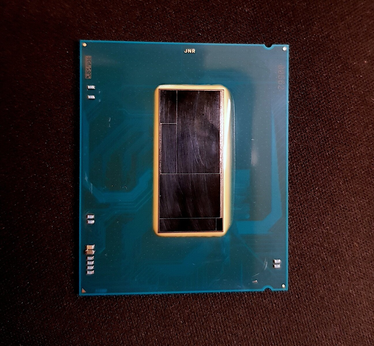
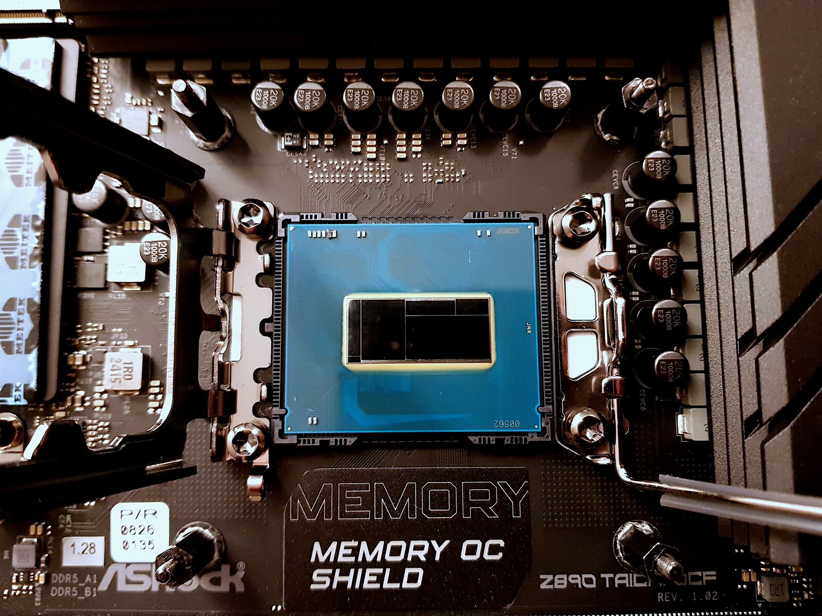
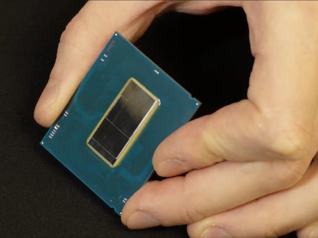
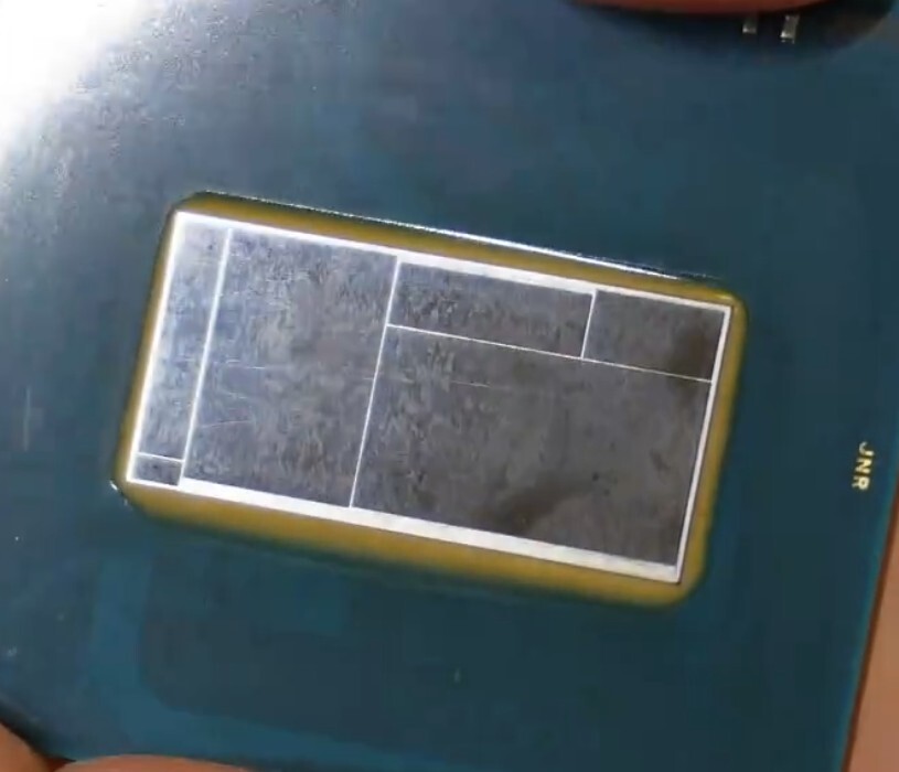
Ahead of its October 23 release, PC enthusiast and Twitch streamer Madness727 released some of the first pictures of a de-lidded Core Ultra "Arrow Lake-S" desktop processor. There's no word on which processor model this is, but it shouldn't matter—all models being released this month are based on the same exact configuration of tiles of the "Arrow Lake-S," which means a Compute tile with an 8P+16E core CPU complex, a Graphics tile with 4 Xe cores, and the larger version of the breakout I/O tile that features an integrated Thunderbolt 4 controller.

Intel already released information on its Core Ultra "Arrow Lake-H" mobile processor that comes out in Q1-2025, which is shown featuring a physically smaller Compute tile that has a 6P+8E core CPU complex, a larger Graphics tile with 8 Xe cores, and a smaller breakout I/O tile. You can see where this is going for some of the cheaper Core Ultra 5 and Core Ultra 3 desktop processor models that release in Q1-2025. De-lidding is the process of removing the integrated heatspreader of a desktop processor to enable direct contact between the chip below, and the cooling solution. It is preferred by professional overclockers that use extreme cooling solutions.


View at TechPowerUp Main Site | Source
 
Looks dangerous to de-lid.
 
It's a miracle that overclocking still exists, even at the professional level. There used to be a period when companies purposely left it open for anyone more capable than a head of cabbage to enjoy a "free" performance boost on purchased hardware.
 
Will I need a new die-mate?

depends on the cpu model, some have liquid metal. Those are harder to delid.
I think you mean soldered ones. You really shouldnt delid those.
 
Looks like somebody made an oopsiedoopsiefuckywucky with the caps during the delid, nice resolder hahaha
 
Molten solder is a liquid metal.

At school you were told that liquid metals are considered, that maintain their liquid state at near room temperatures, quit joking.
 
Last edited:
I don't understand why Intel broke the CPU into so many parts. This is a joke. The IMC is put on the SOC tile for a reason along with various NPUs and media codecs that you will never need, especially on the KF SKU when this is supposed to be a serious processor, not a toy. And now it feels like it's not even the main focus of being a CPU. this has N6 and N5 tiles in it. Intel have a perfectly good N3B SOC GPU chip in Lunar Lake, why not use it, so why are we getting this worse crap with a backport stitched together ghetto style.
 
First they made fun of AMD for glueing multiple chips together and now here we are.
 
First they made fun of AMD for glueing multiple chips together and now here we are.
With the new cooperation between AMD and Intel on x86, I hope this will stop Intel's childish antics and get serious. I have no problem with competitive trash talk but you have to be winning in something to make such comments. Saying Nvidia was 'lucky', TSMC is in a 'conflict region' and AMD 'glues' its chips is not doing Intel any favors but instead makes them look desperate.
 
I don't understand why Intel broke the CPU into so many parts. This is a joke. The IMC is put on the SOC tile for a reason along with various NPUs and media codecs that you will never need, especially on the KF SKU when this is supposed to be a serious processor, not a toy. And now it feels like it's not even the main focus of being a CPU. this has N6 and N5 tiles in it. Intel have a perfectly good N3B SOC GPU chip in Lunar Lake, why not use it, so why are we getting this worse crap with a backport stitched together ghetto style.
Disaggregated manufacturing is exponentially cheaper and more effective than one giant tile. AMD did this with their CCDs - and essentially offered us the first affordable 8 core by gluing 2 quad cores together.

The bigger the die, the bigger the likelihood of failure. So rather than making one giant, super expensive, failure prone chip at 1.8 nm, you can make a bunch of smaller, cheaper dies at 1.8nm and then glue them to the other pieces made at 7/10nm on a more mature process that costs less.

As long as your interconnect is fast enough it's an amazing idea.
Luckily its not really 1.8 nm so its a little easier to make. The smallest feature sizes of any chip is still many ten’s of nanometers.
 
122mm2 CPu 88 SOC. 280 total /w dummy tiles

As long as your interconnect is fast enough it's an amazing idea.
The memory controller is 8mm2, Intel should have at least put it on the CPU tile where it belongs since sandy bridge times.
 
Last edited:
The memory controller is 8mm2, Intel should have at least put it on the CPU tile where it belongs since sandy bridge times.
I don't know about that. AMD didn't put it on the CCX and it seems to work out just fine for them. Also when you consider things like iGPUs and anything that has DMA off of the CPU tile, you're still going to need a wide interconnect to deal with those transfers to and from where ever the CPU's compute (tile or chiplet,) is. It does hurt latency a little bit, but nothing like putting it off package. You introduce latency with distance and the tiles are pretty close together. To be honest, a little more cache can offset something like that.
 
122mm2 CPu 88 SOC. 280 total /w dummy tiles


The memory controller is 8mm2, Intel should have at least put it on the CPU tile where it belongs since sandy bridge times.
the physical connection to the ram brings it's own slowness and doesn't work on the tiny node the cpu tile is made on.
So until they crack how to make the PHY's and controller scale down again it probably more interesting to try and alleviate the tiny bit of extra latency with a sizeable L3
 
This kind of tile-based MCM looks a lot better to me than AMD's chiplets. At least heat is concentrated around the middle of the package, which leaves you with more surface area to dissipate it.

I just still don't like the e-core/p-core thing. I wish 1. Intel will release Bartlett Lake, and/or 2. AMD will implement a similar tile-based design on Zen 6.
 
Back
Top