- Joined
- Oct 9, 2007
- Messages
- 46,390 (7.67/day)
- Location
- Hyderabad, India
| System Name | RBMK-1000 |
|---|---|
| Processor | AMD Ryzen 7 5700G |
| Motherboard | ASUS ROG Strix B450-E Gaming |
| Cooling | DeepCool Gammax L240 V2 |
| Memory | 2x 8GB G.Skill Sniper X |
| Video Card(s) | Palit GeForce RTX 2080 SUPER GameRock |
| Storage | Western Digital Black NVMe 512GB |
| Display(s) | BenQ 1440p 60 Hz 27-inch |
| Case | Corsair Carbide 100R |
| Audio Device(s) | ASUS SupremeFX S1220A |
| Power Supply | Cooler Master MWE Gold 650W |
| Mouse | ASUS ROG Strix Impact |
| Keyboard | Gamdias Hermes E2 |
| Software | Windows 11 Pro |
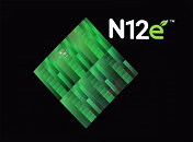
TSMC on Monday announced the N12e silicon fabrication node. An enhancement of its 12 nm FinFET node, N12e is designed for value 5G application processors, MODEMs, and IoT edge devices, such as true-wireless earbuds, smartwatch processors, wearables, VR HMDs, entry-level and mainstream SoCs, etc. The node has been derived from the company's 12FFC+_ULL node, and fits into the 12-16 nm class of nodes. It's intended to succeed the company's 22ULL node (in terms of pricing), offering a 76% increase in logic density, 49% increase in clock speed at a given power, 55% improvement in power draw at a given speed, 50% reduction in SRAM leakage current, and low Vdd, with support for logic voltages as low as 0.4 V. That last bit in particular should make the node suitable for tiny, battery-powered devices such as wearables.

View at TechPowerUp Main Site


View at TechPowerUp Main Site