• Welcome to TechPowerUp Forums, Guest! Please check out our forum guidelines for info related to our community.

AMD EPYC "Bergamo" 128-core Processor Based on Same SP5 Socket as "Genoa"

btarunr

Editor & Senior Moderator
Staff member
Joined
Oct 9, 2007
Messages
47,670 (7.43/day)
Location
Dublin, Ireland
System Name RBMK-1000
Processor AMD Ryzen 7 5700G
Motherboard Gigabyte B550 AORUS Elite V2
Cooling DeepCool Gammax L240 V2
Memory 2x 16GB DDR4-3200
Video Card(s) Galax RTX 4070 Ti EX
Storage Samsung 990 1TB
Display(s) BenQ 1440p 60 Hz 27-inch
Case Corsair Carbide 100R
Audio Device(s) ASUS SupremeFX S1220A
Power Supply Cooler Master MWE Gold 650W
Mouse ASUS ROG Strix Impact
Keyboard Gamdias Hermes E2
Software Windows 11 Pro
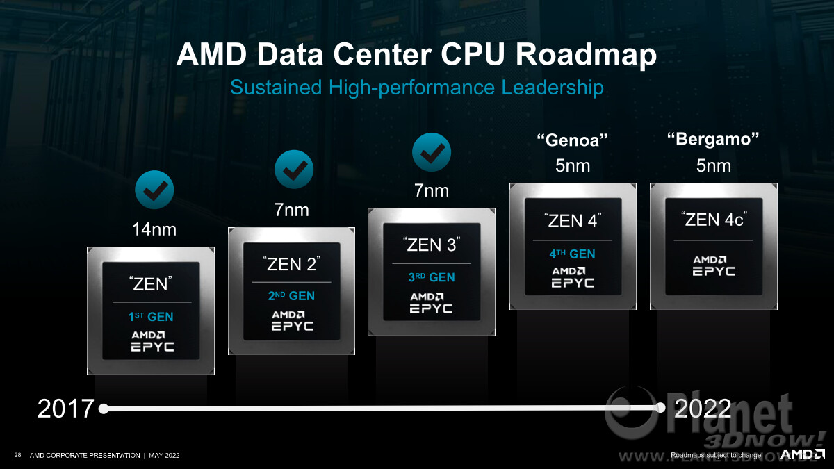
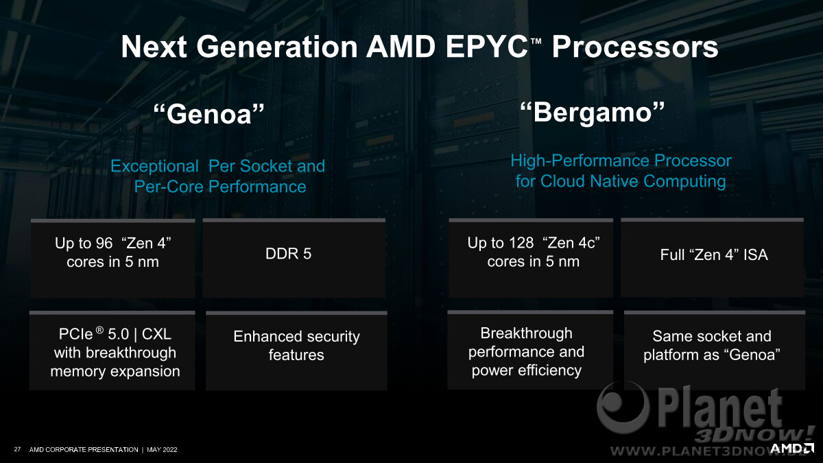
AMD is launching two distinct classes of next-generation enterprise processors, the 4th Generation EPYC "Genoa" with CPU core-counts up to 96-core/192-thread; and the new EPYC "Bergamo" with a massive 128-core/256-thread compute density. Pictures of the "Genoa" MCM are already out in the wild, revealing twelve "Zen 4" CCDs built on 5 nm, and a new-generation sIOD (I/O die) that's very likely built on 6 nm. The fiberglass substrate of "Genoa" already looks crowded with twelve chiplets, making us wonder if AMD needed a larger package for "Bergamo." Turns out, it doesn't.

In its latest Corporate presentation, AMD reiterated that "Bergamo" will be based on the same SP5 (LGA-6096) package as "Genoa." This would mean that the company either made room for more CCDs, or the CCDs themselves are larger in size. AMD states that "Bergamo" CCDs are based on the "Zen 4c" microarchitecture. Details about "Zen 4c" are scarce, but from what we gather, it is a cloud-optimized variant of "Zen 4" probably with the entire ISA of "Zen 4," and power characteristics suited for high-density cloud environments. These chiplets are built on the same TSMC N5 (5 nm EUV) process as the regular "Zen 4" CCDs.


View at TechPowerUp Main Site | Source
 
I wonder if any of this will make it to more cores in the AM5 socket with Zen4, probably not. But, it'd be interesting if a package had one Zen4 chiplet and one Zen4c chiplet... 24 cores/48 threads? Then throw some V-cache in, haha
 
I wonder if any of this will make it to more cores in the AM5 socket with Zen4, probably not. But, it'd be interesting if a package had one Zen4 chiplet and one Zen4c chiplet... 24 cores/48 threads? Then throw some V-cache in, haha
I hope they pull something special out of the bag as my old Threadripper 2950X is getting a bit old now; a 2018 build should have been upgraded last year...
 
this comparable to E-cores of Intel.
E-core does not have the same ISA as the P-cores
Things running fine on P-cores might crash on e-cores.

But things running fine on Zen4 will run fine on Zen4c, just a bit slower without a larger cache.
 
E-core does not have the same ISA as the P-cores
Things running fine on P-cores might crash on e-cores.

But things running fine on Zen4 will run fine on Zen4c, just a bit slower without a larger cache.
The other thing AMD could do is use higher density cell libraries for Zen4c, reducing the size and power requirements of each core but at the expense of reduced frequency scaling (and hence processing power). That way they can also maintain the same ISA, avoiding the issues Intel has with AVX512 support on Alder Lake, while still scaling down core size and power in order to scale up core count. Likely we'll see both, reduced L2/L3 cache and higher density cell libraries.
 
Then the 3D cache enters the equation, fixing the deficiency if necessary to combat the avalanche of small cores that intel intends to use. Well done.
Current Zen3 CCD uses half of its die area for L3 cache
Imagine all of those areas can be ultilize to fit double the cores and L3 cache is just added by stacking V-cache vertically.
That means a 16 core CCD within the same area......
 
Four CCDs in a row ain't gonna work in the same socket.

1653582458209.png


I guess they'll cluster them in 2x2 quads - something like this, though they'll probably do it more carefully than the 90 seconds it took me to photoshop that dog's dinner.
 
Current Zen3 CCD uses half of its die area for L3 cache
Imagine all of those areas can be ultilize to fit double the cores and L3 cache is just added by stacking V-cache vertically.
That means a 16 core CCD within the same area......
I don't think it's possible to drop all the L3 cache, then just add 3D cache on top. from what I saw the extra memory die is stacked above the normal cache.

1068823312a_575px.jpg
 
I don't think it's possible to drop all the L3 cache, then just add 3D cache on top. from what I saw the extra memory die is stacked above the normal cache.

View attachment 248909
Yep, I believe it was mentioned in the 3D-VCache announcement last year that a big reason they can stack above the existing cache is because cache logic generates less heat than the execution pipelines. If there was execution logic underneath instead of more cache, the thermals would be unmanageable without massively throttling the clockspeeds.
 
128-core/256-thread compute density
Imagine a two processor server having 512 logical threads. What a time to be alive.
 
Imagine a two processor server having 512 logical threads. What a time to be alive.
Twelve memory channels (12 x 64 bits) may soon become a limiting factor in such big processors, depending on the application of course.
 
Twelve memory channels (12 x 64 bits) may soon become a limiting factor in such big processors, depending on the application of course.
Genoa/Bergamo has 12-channel DDR5 (that's 24 x 40 bits).
 
Back
Top