• Welcome to TechPowerUp Forums, Guest! Please check out our forum guidelines for info related to our community.

AMD Sets RV775 to Chase Down G200b?

btarunr

Editor & Senior Moderator
Staff member
Joined
Oct 9, 2007
Messages
47,670 (7.43/day)
Location
Dublin, Ireland
System Name RBMK-1000
Processor AMD Ryzen 7 5700G
Motherboard Gigabyte B550 AORUS Elite V2
Cooling DeepCool Gammax L240 V2
Memory 2x 16GB DDR4-3200
Video Card(s) Galax RTX 4070 Ti EX
Storage Samsung 990 1TB
Display(s) BenQ 1440p 60 Hz 27-inch
Case Corsair Carbide 100R
Audio Device(s) ASUS SupremeFX S1220A
Power Supply Cooler Master MWE Gold 650W
Mouse ASUS ROG Strix Impact
Keyboard Gamdias Hermes E2
Software Windows 11 Pro
Sources tell Expreview that AMD is working on a new graphics processor (apart from the mysterious RV790), as an immediate reaction to the 55nm high-end GPUs NVIDIA is set to release. NVIDIA on its part is working on GeForce GTX 260 (55nm), GeForce GTX 285 (successor to GeForce GTX 280) and the dual-GPU monstrosity, GeForce GTX 295. To rival this, according to the source, AMD is working on the RV775 and derivatives based on its yields' performance.

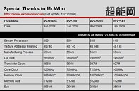
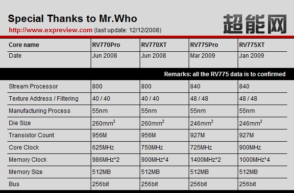
These GPUs are slated for January thru March 2009. It has some very interesting specifications. To begin with, 840 stream processors. While stream processors on a current generation RV770 cannot be added/subtracted in quantities of 40 stream processors, perhaps, the increment of 40 SPs is derived from an extra ALU cluster the RV770 comes with by default (which helps in die harvesting, where the spare ALU cluster makes up for any damaged cluster, thereby improving yields). This would require near-perfect GPUs in the making (if re-engineering of the RV770 on a large scale is to be avoided). Another interesting point is regarding the smaller die. At this point we are clueless as to how that is possible without re-engineering the RV770 at a large scale. Treat yourselves to the specifications meanwhile:


View at TechPowerUp Main Site
 
Last edited:
Unreliable sources tell Expreview that AMD is working on a new graphics processor:roll:
 
Unreliable sources tell Expreview that AMD is working on a new graphics processor:roll:

Changed to unknown. Been using "unreliable" in the wrong context. :o
 
More shaders and a smaller die?
 
More shaders and a smaller die?

The only explanation that i can see for a smaller die with more shader clusters is, that the yields must be so high and perfect after producing so many cores on 55nm process, that ATI is confident now to put lesser or maybe no spare shader clusters in the die for die harvesting
 
Changed to unknown. Been using "unreliable" in the wrong context. :o

unknown = unreliable when it comes to the internet:)
This could be true. Maybe the ripped anything not gaming related and made just a pure gaming card.
 
More shaders and a smaller die?

While the RV770 comes in 800 / 640 (and lol 560) SP configurations, physically the die could be having more than 800 SPs (> 10 ALU clusters). These are spare components that AMD activates to replace damaged/dysfunctional ALU clusters (and increase yields). About the "smaller die" part, I'm just as clueless as you are.
 
That number is strange. AFAIK RV770 comes with one extra Shader Processor per cluster, that is 17 instead of the 16. 10 clusters x 16 SP x 5 ALU = 800 AND 17 x 10 x 5 = 850, not 840. Maybe just a typo when the mysterious source sent the info.

Anyway IMO this is false or just some kind of viral marketing to the RV790 or is the RV790 in any case. BUt BOTH won't be released IMO.
 
ohh i see the most impressive thing amd add more 8 texture unit , that's nice , and also i see amd back to old names pro and xt , and see the hell rv775xt have 900mhz core speed , dumm , and what about overclock did i expect to see first gpu run at 1ghz
 
Last edited:
There are some issues in the table, which may be causing confusion for us:

RV770 has 956 million transistors according to some sites, and 965 million according to others. Somewhere there is a typo. Let's assume 956 is correct since this is the most popular, then

How would ATI REDUCE the number of transistors whilst INCREASING the number of shaders. What is being changed here? Unless there is another typo and they are increasing the transistor count and going from 55nm to 50 nm. OR they are reducing voltage and increasing the density WITHIN 55nm scale to get the same or more transistors in a smaller space. BUT that is a major tape-out redesign issue.

The table and the technology and the statement no major redesign is mutually inconsistent.

***

What I dont like is that for ATI/AMD shaders are NOT the bottleneck, but TMU and ROPs are: see http://forums.techpowerup.com/showthread.php?p=1062008.
Therefore meh! They are adding something that doesnt add performance value. :pimp: They are "fixing" the wrong end of the stick.
 
Do you guys know when will the CrossFire Sideport on HD 4870 X2 be enabled.
 
or on a 4850 :( my 790GX board only will let me use side port memory with a X something
 
What I dont like is that for ATI/AMD shaders are NOT the bottleneck, but TMU and ROPs are: see http://forums.techpowerup.com/showthread.php?p=1062008.
Therefore meh! They are adding something that doesnt add performance value. :pimp: They are "fixing" the wrong end of the stick.

I think the key "improvement" would be the 900 MHz clock + 20% more ROPs (not too shabby, I'd say). Besides, 40 more shaders seems unlikely (1 SIMD is 16x5=80 SPUs). They could also ditch the sideport, which is not used at all and save some space on that. All in all, I don't think the info is reliable.
 
The table and the technology and the statement no major redesign is mutually inconsistent.

Agreed. I firstly didn't notice there were 48 texture units. That makes my typo theory impossible. That would mean either they did a mayor redesign to the SP/TMU clusters or that they added 2 clusters. In any case numbers don't fit or are inconsistent to the statement no major redesign.

12 clusters x 14 SP x 5 ALU = 840 SP???
 
900MHz core clock O.o wow... I hate to say it but DO WANT
 
i would lean more towards them releasing sub par numbers under what is really going to be released
remember last time they where saying 400 sp's or 600 or whatever, and it turned out to be 800, does anyone else make this connection ?
 
i would lean more towards them releasing sub par numbers under what is really going to be released
remember last time they where saying 400 sp's or 600 or whatever, and it turned out to be 800, does anyone else make this connection ?

Yeah but back then they were posting numbers that made sense. This ones scream "we are FAKE" so what's the point??
 
AMD/ATi are working on something ofcourse, now if its this new 775 then good for them, but i dont think so. With less then 2 months to go, things would have been a little more clearer, like the 295GTX - already pictures of the completed card are circulating.
 
or on a 4850 :( my 790GX board only will let me use side port memory with a X something

Dunno what your talking about, on a 790GX you can only use the card by it self, or the 128mb side port (HD3300) by itself you can't do crossfire between the two because the cores are different.

It looks like ATI will do the same thing as they did with the hd3000 series.

with the old r600 it encompases every card from hd2000 series through the hd3000 series,

I got this gut feeling these will get dubbed radeon 4900 series or 4890 or something of that nature.
 
Thanks for putting this discussion to rest. Funny that fudzilla calls hoax! LOL
 

Cool, that means nothing really new from ATi until late 2009, hopefully nVidia will follow the trend(after G200b of course). Maybe it is just me, but I miss the days were we would see some time between major releases. I would like to actually keep the same graphics card in my machine for at least a year. I haven't done that since my 7900GT's, and I was hoping the upgrade to G200b would hold me over for a year.
 
Back
Top