• Welcome to TechPowerUp Forums, Guest! Please check out our forum guidelines for info related to our community.

AMD Strix Point SoC "Zen 5" and "Zen 5c" CPU Cores Have 256-bit FPU Datapaths

btarunr

Editor & Senior Moderator
Staff member
Joined
Oct 9, 2007
Messages
47,670 (7.43/day)
Location
Dublin, Ireland
System Name RBMK-1000
Processor AMD Ryzen 7 5700G
Motherboard Gigabyte B550 AORUS Elite V2
Cooling DeepCool Gammax L240 V2
Memory 2x 16GB DDR4-3200
Video Card(s) Galax RTX 4070 Ti EX
Storage Samsung 990 1TB
Display(s) BenQ 1440p 60 Hz 27-inch
Case Corsair Carbide 100R
Audio Device(s) ASUS SupremeFX S1220A
Power Supply Cooler Master MWE Gold 650W
Mouse ASUS ROG Strix Impact
Keyboard Gamdias Hermes E2
Software Windows 11 Pro
AMD in its architecture deep-dive Q&A session with the press, confirmed that the "Zen 5" and "Zen 5c" cores on the "Strix Point" silicon only feature 256-bit wide FPU data-paths, unlike the "Zen 5" cores in the "Granite Ridge" Ryzen 9000 desktop processors. "The Zen 5c used in Strix has a 256-bit data-path, and so does the Zen 5 used inside of Strix," said Mike Clark, AMD corporate fellow and chief architecture of the "Zen" CPU cores. "So there's no delta as you move back and forth [thread migration between the Zen 5 and Zen 5c complexes] in vector throughput," he added.

It doesn't seem like AMD disabled a physically available feature, but rather, the company developed a variant of both the "Zen 5" and "Zen 5c" cores that physically lack the 512-bit data-paths. "And you get the area advantage to be able to scale out a little bit more," Clark continued. This suggests that the "Zen 5" and "Zen 5c" cores on "Strix Point" are physically smaller than the ones on the 4 nm "Eldora" 8-core CCD that is featured in "Granite Ridge" and some of the key models of the upcoming 5th Gen EPYC "Turin" server processors.


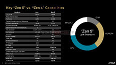
One of the star-attractions of the "Zen 5" microarchitecture is its floating-point unit, which supports AVX512 with a full 512-bit data path. In comparison, the previous-generation "Zen 4" handled AVX512 using a dual-pumped 256-bit FPU. The new 512-bit FPU, depending on the exact workload and other factors, is about 20-40% faster than "Zen 4" at 512-bit floating-point workloads, which is why "Zen 5" is expected to post significant gains in AI inferencing performance, as well as plow through benchmarks that use AVX512.

We're not sure how the lack of a 512-bit FP data-path affects performance of instructions relevant to AI acceleration, since "Strix Point" is mainly being designed for Microsoft Copilot+ ready AI PCs. It's possible that AVX512 and AVX-VNNI are being run on a dual-pumped 256-bit data-path similar to how it is done on "Zen 4." There could be some performance/Watt advantages to doing it this way, which could be relevant to mobile platforms.

View at TechPowerUp Main Site
 
That is going to be nasty in the future when there is no feature parity and software that runs fine on zen5 desktop that won’t be running on zen 5 laptop/mini/aio
 
That is going to be nasty in the future when there is no feature parity and software that runs fine on zen5 desktop that won’t be running on zen 5 laptop/mini/aio
There's no incompatibility here.
All Zen 5/5c cores support the exact same instructions. It's only the internal execution pipeline that's fully 512-bit wide on desktop/server variants and "2x256"-bit on mobile. With the latter being very close to what Zen 4/4c was doing I suppose.
 
There's no incompatibility here.
All Zen 5/5c cores support the exact same instructions. It's only the internal execution pipeline that's fully 512-bit wide on desktop/server variants and "2x256"-bit on mobile. With the latter being very close to what Zen 4/4c was doing I suppose.
Sure and in say 5 years or so, some very popular software is going to need the full 512 to fully function and the double pumped one isn't going to be enough.
I was seriously bummed out as a kid when my 486SX2 wouldn't play quake
 
Sure and in say 5 years or so, some very popular software is going to need the full 512 to fully function and the double pumped one isn't going to be enough.
I was seriously bummed out as a kid when my 486SX2 wouldn't play quake
486SX couldn't run Quake because it was a processor without a FPU, so it was unable to execute x87 instructions needed by the game.
In this situation all Zen 5 variants support the same instruction sets including AVX-512. From software perspective there is no difference between them other than execution speed.
 
Sure and in say 5 years or so, some very popular software is going to need the full 512 to fully function and the double pumped one isn't going to be enough.
I was seriously bummed out as a kid when my 486SX2 wouldn't play quake

First, no developer making a mass-market app is going to develop a product with AVX 512 support and not have a fall back implementation. Not unless you are talking something very niche where the dev knows people who use their app all have newer hardware. There will still be a significant chunk of users without AVX 512 support in 5 years, devs won't just up an abandon them.

Second, people using CPUs with double pumped AVX 512 do in fact have AVX 512 support. They will be able to use the app unlike in your scenario where you could not play quake. Double pumped AVX512 is pretty performant on Zen 4 processors and I expect the same to apply to these mobile processors as well.

The mobile CPUs being double-pumped is a non-issue for compatibility.
 
Last edited:
Considering how AMD put in the Geekbench AES benchmark to calculate that IPC increase, this change will probably have a pretty signficant decrease if you were to calculate the IPC from the same benchmarks as AMD did.
 
Sure and in say 5 years or so, some very popular software is going to need the full 512 to fully function and the double pumped one isn't going to be enough.
This won't be the case, to software there is no detectable difference, these are the exact same instructions. It's just that the 512-bit datapath runs faster than the other (not by a factor of 2)
 
Sure and in say 5 years or so, some very popular software is going to need the full 512 to fully function and the double pumped one isn't going to be enough.
I was seriously bummed out as a kid when my 486SX2 wouldn't play quake
I think you're more likely to run into some app that won't run without an NPU, but even that should fall back to the GPU in a pinch. I can't imagine any popular software targeting specific hardware, especially something like AVX512, where desktop Intel processors since Adler Lake don't support that feature at all. It's coming back again, but talk about a setback if you're hoping for popular consumer adoption.
 
The AVX512 units don't only perform FP operations but also integer and bitwise operations on vectors. I don't know enough to judge but those may have a bigger impact on games and other consumer workloads than FP operations if the performance is halved or significantly reduced. Integer math is used everywhere, FP math has a narrower range of usability.
 
The AVX512 units don't only perform FP operations but also integer and bitwise operations on vectors. I don't know enough to judge but those may have a bigger impact on games and other consumer workloads than FP operations if the performance is halved or significantly reduced. Integer math is used everywhere, FP math has a narrower range of usability.
Current benchmark results seem to point towards games and consumer workloads not making good use of such features anyway, outside a few exceptions. But the capability had to be there first. Capability one of the major makes is no longer (or not yet with AVX10) providing.

I think applications making really good use of AVX512 tends to be memory bandwidth bound, if not load/store bound, on current consumer hardware, anyway.

Back on topic, I wonder whether it had anything to do with more than power consumption and efficiency, and whether there would be a separate moniker for these reduced cores.
 
The AVX512 units don't only perform FP operations but also integer and bitwise operations on vectors. I don't know enough to judge but those may have a bigger impact on games and other consumer workloads than FP operations if the performance is halved or significantly reduced. Integer math is used everywhere, FP math has a narrower range of usability.

Is there really that much significance in this difference of true AVX-512 capability vs. AVX-512 on 256-bit hardware? APU dies were born with and have never escaped the half L3 curse. We have already been expecting poorer CPU performance in all aspects from them every year since 2017, so this is just more of the same.
 
If AMD put the memory controller on the same die of the x86 cores, I think Ryzen CPUs would have a performance gain of around 20%.
73LyGP5.png
 
If AMD put the memory controller on the same die of the x86 cores, I think Ryzen CPUs would have a performance gain of around 20%.
73LyGP5.png
Even if true this design would 100% go against the chiplet design. The whole reason why the controller is separate is because the cores are the same between varying different product stacks. The Memory controller and I/O die are the only changes "more complicated than that, but for simplicity" between the different product stacks.
 
Even if true this design would 100% go against the chiplet design. The whole reason why the controller is separate is because the cores are the same between varying different product stacks. The Memory controller and I/O die are the only changes "more complicated than that, but for simplicity" between the different product stacks.
I know that, but AMD is already making several different core configurations. And they may have already developed (AI) apps that do much of the chip design work in a few minutes or hours, work that used to take several months.

With the memory controller integrated on the same die of the x86 cores, the x86 cores would have a much lower RAM access latency and, thus, the chip's IPC would increase.
This is speculation but i will assume its not worth it finically compared to how flexible their product stack is now.
 
Back
Top