• Welcome to TechPowerUp Forums, Guest! Please check out our forum guidelines for info related to our community.

AMD Zen 5 Microarchitecture Referenced in Leaked Slides

btarunr

Editor & Senior Moderator
Staff member
Joined
Oct 9, 2007
Messages
47,670 (7.43/day)
Location
Dublin, Ireland
System Name RBMK-1000
Processor AMD Ryzen 7 5700G
Motherboard Gigabyte B550 AORUS Elite V2
Cooling DeepCool Gammax L240 V2
Memory 2x 16GB DDR4-3200
Video Card(s) Galax RTX 4070 Ti EX
Storage Samsung 990 1TB
Display(s) BenQ 1440p 60 Hz 27-inch
Case Corsair Carbide 100R
Audio Device(s) ASUS SupremeFX S1220A
Power Supply Cooler Master MWE Gold 650W
Mouse ASUS ROG Strix Impact
Keyboard Gamdias Hermes E2
Software Windows 11 Pro
A couple of slides from AMD's internal presentation were leaked to the web by Moore's Law is Dead, referencing what's allegedly the next-generation "Zen 5" microarchitecture. Internally, the performance variant of the "Zen 5" core is referred to as "Nirvana," and the CCD chiplet (CPU core die) based on "Nirvana" cores, is codenamed "Eldora." These CCDs will make up either the company's Ryzen "Granite Ridge" desktop processors, or EPYC "Turin" server processors. The cores themselves could also be part of the company's next-generation mobile processors, as part of heterogenous CCXs (CPU core complex), next to "Zen 5c" low-power cores.

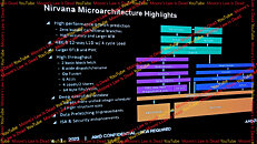
In broad strokes, AMD describes "Zen 5" as introducing a 10% to 15% IPC increase over the current "Zen 4." The core will feature a larger 48 KB L1D cache, compared to the current 32 KB. As for the core itself, it features an 8-wide dispatch from the micro-op queue, compared to the 6-wide dispatch of "Zen 4." The integer execution stage gets 6 ALUs, compared to the current 4. The floating point unit gets FP-512 capabilities. Perhaps the biggest announcement is that AMD has increased the maximum cores per CCX from 8 to 16. At this point we don't know if it means that "Eldora" CCD will have 16 cores, or whether it means that the cloud-specific CCD with 16 "Zen 5c" cores will have 16 cores within a single CCX, rather than spread across two CCXs with smaller L3 caches. AMD is leveraging the TSMC 4 nm EUV node for "Eldora," the mobile processor based on "Zen 5" could be based on the more advanced TSMC 3 nm EUV node.


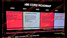
The opening slide also provides a fascinating way AMD describes its CPU core architectures. According to this, "Zen 3" and "Zen 5" are new cores, while "Zen 4" and the future "Zen 6" cores are leveraged cores. If you recall, "Zen 3" had provided a massive 19% IPC uplift over "Zen 2," which helped AMD dominate the CPU market. Although with a more conservative 15% IPC gain estimate over "Zen 4," the "Zen 5" core is expected to have as big of an impact on AMD's competitiveness.

Speaking of the "Zen 6" microarchitecture and the "Morpheus" core, AMD is anticipating a 10% IPC increase over "Zen 5," new FP16 capabilities for the core, and a 32-core CCX (maximum core-count). This would see a second round of significant increases in CPU core counts.

Diving deep into the "Zen 5" core, and we see AMD introduce an even more advanced branch prediction unit. If you recall, branch predictor improvements had the largest contribution toward the generational IPC gain of "Zen 4." The new branch predictor comes with zero bubble conditional branches capabilities, accuracy improvements, and a larger BTB (branch target buffer). As we mentioned, the core has a larger 48 KB L1D cache, and an unspecified larger D-TLB. There are throughput improvement across the front-end and load/store stages, with dual basic block fetch units, 8-wide op dispatch/rename; Op Fusion, a 50% increase in ALCs, a deeper execution window, a more capable prefetcher, and updates to the CPU core ISA and security. The dedicated L2 cache per core remains 1 MB in size.

View at TechPowerUp Main Site | Source
 
Hmmm, was hoping for more TBH. I don't know how Zen5 or Zen6 is going to compete against intel's new architecture, if that ever actually comes out.

I still think AMD should be putting more on the CPU die and put an end to this L3 cache starved design. Zen clearly needs more L3 to work properly, and this situation with the glued on L3 is silly. At first it was great, and a novel approach, 2nd time was a little weird, but still fine, but going into the 3rd gen of this, it's clear that it's just a money-making racket, and that the CPU needs this extra cache to work properly. Zen6 will really need a larger L2 cache too, as a 10% IPC increase will be insufficient to counter Intel. Doubling of L2 cache is worth 3-5% IPC uplift, too much to be ignored if all your offering is a 10% uptick. AMD needs at least a 15% IPC uptick each generation.

Quad channel memory support on the Desktop is really needed if we are looking at the possibility of 32 cores on the desktop. AMD's DDR5 memory controller is crap compared to Intel's, so another thing for AMD to fix.
No, it's actually brilliant if it still works. The caches have almost no reduction between processes, the 3D cache is 6nm ($9k per wafer)
while the chip is produced in 5nm (U$ 17k), they should use even more with 3nm as the yield per wafer is well below expectations

I just wanted to see dual channel(128bit) per module :P
.
 
Wasn't it supposed to exceed (internal?) expectations or has WTFtech on YT revised his own targets, again :wtf:

10-15% isn't exactly ground breaking!
 
So many codenames for a single architecture! :wtf:

Hmmm, was hoping for more TBH. I don't know how Zen5 or Zen6 is going to compete against intel's new architecture, if that ever actually comes out.

I still think AMD should be putting more on the CPU die and put an end to this L3 cache starved design. Zen clearly needs more L3 to work properly, and this situation with the glued on L3 is silly. At first it was great, and a novel approach, 2nd time was a little weird, but still fine, but going into the 3rd gen of this, it's clear that it's just a money-making racket, and that the CPU needs this extra cache to work properly. Zen6 will really need a larger L2 cache too, as a 10% IPC increase will be insufficient to counter Intel. Doubling of L2 cache is worth 3-5% IPC uplift, too much to be ignored if all your offering is a 10% uptick. AMD needs at least a 15% IPC uptick each generation.

Quad channel memory support on the Desktop is really needed if we are looking at the possibility of 32 cores on the desktop. AMD's DDR5 memory controller is crap compared to Intel's, so another thing for AMD to fix.
It's a great design in terms of flexibility. If you need clock speed, you go with a normal CPU. If you need cache, you buy an X3D.

It must be wrong or outdated, it says 2023...
Possibly. We know MLID and their "leaks".
 
He's entertaining and way better than the nVidia fanboys or those with super egos.
Clowns are entertaining, but I don't turn to them for news.
 
I guess AMD is going to move to 2 CCD designs even for mid range and up, to negate Intel's core advantage. So, a future gaming CPU could have an 8/16 core CCD and 3D cache on it, with typical Zen cores and an extra 8/16 CCD with Zenc cores for that extra core count that is absolutely needed to sell CPUs today.
 
MLID tho...
A yes yes. If a leaker gets something right everyone promply forgets it or calls it a lucky guess.
If a leaker gets something wrong it hangs over them for the rest of time like badge of shame and reason not to trust anything they say, ever.
It must be wrong or outdated, it says 2023...
Tapeout.
Hmmm, was hoping for more TBH. I don't know how Zen5 or Zen6 is going to compete against intel's new architecture, if that ever actually comes out.
Both are pretty competitive. At least on desktop and mobile. Less so on worstation and server. And if what ever comes out?
and that the CPU needs this extra cache to work properly.
Not true. Extra L3 can benefit some workloads more than others but more L3 is not universally faster.
Zen6 will really need a larger L2 cache too, as a 10% IPC increase will be insufficient to counter Intel.
There is a balance beteween cache size and latency. The bigger the cache, the higher the latency.
Cache increases need to be worked in to design to minimize adverse effects from size increase.
AMD needs at least a 15% IPC uptick each generation.
Based in Intel's fairy tale leaks?
Quad channel memory support on the Desktop is really needed if we are looking at the possibility of 32 cores on the desktop. AMD's DDR5 memory controller is crap compared to Intel's, so another thing for AMD to fix.
Never going to happen. Quad channel will not come to mainstream. Id say AMD's memory controller is better actually. Atleast there you can run 8000 stable where as with Intel its tough even for experts to get it stable.
Clowns are entertaining, but I don't turn to them for news.
What kind on "news"? The only way this gets more official is if AMD themselves comes out and confirms it which is never gonna happen.
At best we can expect some sort of teaser for Zen 5 during CES 2024 in January.
 
No, it's actually brilliant if it still works. The caches have almost no reduction between processes, the 3D cache is 6nm ($9k per wafer)
while the chip is produced in 5nm (U$ 17k), they should use even more with 3nm as the yield per wafer is well below expectations

I just wanted to see dual channel(128bit) per module :p
.
That N5 figure is wildly off the mark. A N3 wafer is estimated to cost Apple $16000 to $17000 when yields improve to the point that Apple isn't only paying for working dies.
 
That N5 figure is wildly off the mark. A N3 wafer is estimated to cost Apple $16000 to $17000 when yields improve to the point that Apple isn't only paying for working dies.
We think TSMC will move to normal wafer-based pricing on N3 with Apple during the first half of 2024, at around $16-17K average selling prices,”

Really ? Would you put your money on this? Let's think, Apple depends on iPhone sales... and TSMC has no competition, so there are no options, TSMC can charge whatever it wants and Apple cannot say "no, I'm not going to pay that and I'm going to manufacture my processors at Samsung or intel and lose 30-40% efficiency." it makes no sense.
We don't know the details of the contracts between Apple and TSMC. Without Apple, TSMC's N3 isn't in good enough shape for other customers:
Apple will pay TSMC for known good die rather than standard wafer prices, at least for the first three to four quarters of the N3 ramp as yields climb to around 70%, Brett Simpson, senior analyst at Arete Research, said in a report provided to EE Times.
A yield of 70% for a 100 to 110 mm^2 die is abysmal. Only small dies like the Ryzen CCDs would yield relatively well with such a process. The GB102, assuming it's the same size as the AD102, would yield only 15 fully functional dies. SRAM redundancy would increase that figure, but it would still be terrible. As far as the ridiculous pricing for N5 is concerned, think about it; it's purported to be doubled over N6/N7 while the process doesn't offer anything like doubled density. It also doesn't line up with what AMD shared during the RDNA3 presentation.

1695996328695.png


As far as Zen 5 is concerned, given the list of improvements, a 10% increase in IPC seems rather low. Zen 4 didn't do as many changes and still managed an average of 13%.
 
Last edited:
i wouldn't be surprised if they remove the L3 cache from the die and move it to a dedicated silicon with the 16 cores and 32 cores CCD. Like Denver said, Cache barely scale with newer process so if they want to keep a similar amount of cache per cores.

Another advantages of having a dedicated die for cache is they are able to squeeze more into the same area since you can use a different libraries.

The IPC gains aren't incredible, but they aren't that bad too. the key thing is the cadence they release, if they get it every 12-18 month, they should remain competitive.
Wouldn't detaching L3 cache make latency much worse though? There could be an off-CCD shared L4 cache, though, much alike Intel is rumoured to use.
 
Wouldn't detaching L3 cache make latency much worse though? There could be an off-CCD shared L4 cache, though, much alike Intel is rumoured to use.
Moving L3 to a separate chiplet is only possible with 3D stacking and TSVs. The additional latency is rather negligible in that case: 3 to 4 cycles for Milan X. We all know the benefits and drawbacks of this approach so this is unlikely to happen unless they use an active interposer à la the MI300.
 
MLID is not a reliable source..period.

Edit: Somebody is having fun, on multiple sites and sources, with the definition of and counts related to CCX and CCD.

BUBBA!
 
Last edited:
Moving L3 to a separate chiplet is only possible with 3D stacking and TSVs. The additional latency is rather negligible in that case: 3 to 4 cycles for Milan X. We all know the benefits and drawbacks of this approach so this is unlikely to happen unless they use an active interposer à la the MI300.
Wait, wasn't the proposed scenario that a separate L3 cache chiplet is not a stacked cache like we have with the X3D processors, thus detaching it from the CCD's? Or did I make some wild assumptions on my own interpretation?
 
Wait, wasn't the proposed scenario that a separate L3 cache chiplet is not a stacked cache like we have with the X3D processors, thus detaching it from the CCD's? Or did I make some wild assumptions on my own interpretation?
@Punkenjoy would know, but I don't think you had the wrong impression. I only pointed out that using that would only be feasible with 3D stacking and TSVs. In other cases, the latency hit and additional power cost would be too high.
 
Previous rumors was for+20-30% IPC. Will see when released.
A 20-30% Single Thread performance gain could be obtained with some clock gain with these IPC gains.

@Punkenjoy would know, but I don't think you had the wrong impression. I only pointed out that using that would only be feasible with 3D stacking and TSVs. In other cases, the latency hit and additional power cost would be too high.

I think like you but i don't really know the real data. It seem to make sense on the surface but we have to remember that AMD now have the Infinity cache on RDNA3 in the MCD modules and not on the main die. They still have plenty of bandwidth but not sure about the latency. GPU are less sensitives to latency than CPU.

I think from what i know that the best options would be to have a cache die on top or bellow a CCD using TSV. But we could be surprised. I would be surprised if it's in the I/O die because currently, there is really not enough bandwidth between a CCD and the I/O die to support that. But if they have a new I/O die (Witch i think, from rumors they won't) they could increase the size of the infinity fabric link and maybe put cache there. The thing is that would make that I/O die even bigger reducing the yield of it and maybe killing it's main benefits.

Also i am not sure if there is enough space on the die to put a dedicated cache die that is not stacked. but who know ! i would be very surprised.
 
Last edited:
Clowns are entertaining, but I don't turn to them for news.
He has good content as well, some of the guests are great. Plus unlike the nVidia fanboys/marketing division or the oversized egos YouTubers he doesn't spread lies, leaks are leaks and should be taken with a grain of salt.
 
A yes yes. If a leaker gets something right everyone promply forgets it or calls it a lucky guess.
If a leaker gets something wrong it hangs over them for the rest of time like badge of shame and reason not to trust anything they say, ever.

Ermm yeah, that is how that works, if you do well, you are just doing your job, if you do wrong, you get fired.....welcome to the real world?
Heck If anything I wish the world had more consequences for ffing up.
 
Back
Top