• Welcome to TechPowerUp Forums, Guest! Please check out our forum guidelines for info related to our community.

AMD's Lisa Su Confirms Zen 4 is Using Optimised TSMC 5 nm Node, 2D and 3D chiplets

TheLostSwede

News Editor
Joined
Nov 11, 2004
Messages
18,475 (2.47/day)
Location
Sweden
System Name Overlord Mk MLI
Processor AMD Ryzen 7 7800X3D
Motherboard Gigabyte X670E Aorus Master
Cooling Noctua NH-D15 SE with offsets
Memory 32GB Team T-Create Expert DDR5 6000 MHz @ CL30-34-34-68
Video Card(s) Gainward GeForce RTX 4080 Phantom GS
Storage 1TB Solidigm P44 Pro, 2 TB Corsair MP600 Pro, 2TB Kingston KC3000
Display(s) Acer XV272K LVbmiipruzx 4K@160Hz
Case Fractal Design Torrent Compact
Audio Device(s) Corsair Virtuoso SE
Power Supply be quiet! Pure Power 12 M 850 W
Mouse Logitech G502 Lightspeed
Keyboard Corsair K70 Max
Software Windows 10 Pro
Benchmark Scores https://valid.x86.fr/yfsd9w
Anandtech asked AMD during a meeting at CES about the production nodes used to make its chips at TSMC and the importance of leading edge nodes for AMD to stay competitive, especially in light of the cost of using said nodes. Lisa Su confirmed in her answer to Anandtech that AMD is using an optimised high-performance 5 nm node for its upcoming Zen 4 processor chiplets, which there interestingly appears to be both 2D and 3D versions of. This is the first time we've heard a mention of two different chiplet types using the same architecture and it could mean that we get to see Zen 4 based CPUs with and without 3D cache.

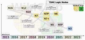
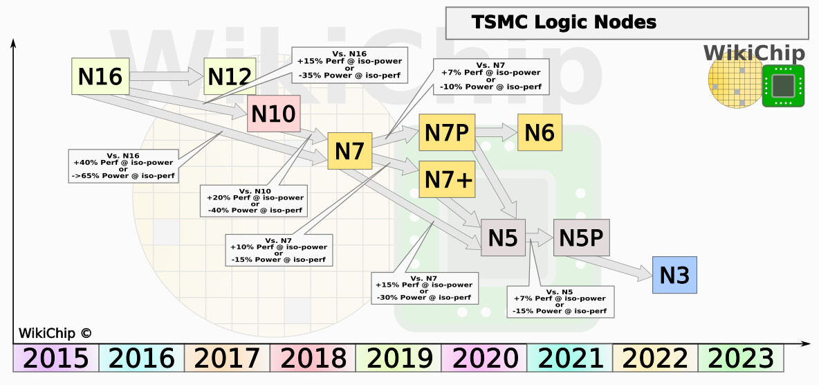
What strikes us as a bit odd about the Anandtech article, is that they mention the fact that several of TSMC's customers are already making 4 nm and soon 3 nm chips and are questioning why AMD wouldn't want to be on these same nodes. It seems like Anandtech has forgotten that not all process nodes are universally applicable and just because you can make one type of chip on a smaller node, doesn't mean it'll be suitable for a different type of chip. For the longest of times, mobile SoCs or other similar chips seem to always have been among the first things being made on new nodes, with more complex things like GPUs and more advanced CPUs coming later, to tweaked versions of the specific node. The fact that TSMC has no less than three 7 nm nodes, should be reason enough to realise that the leading edge node might not be the ideal node for all types of chips.


In related news, TSMC is said to have accepted advanced payments of US$5.44 billion from at least 10 of its clients, of which AMD, Apple, Nvidia and Qualcomm are all mentioned. The payments have been done to secure production capacity, although for exactly how long time into the future isn't clear. TSMC saw advanced payments of US$3.8 billion in the first three quarters of last year and it's likely that these kinds of deals will continue as long as there's more demand than supply.

View at TechPowerUp Main Site
 
So the 2 different chiplets with vcache and without are a thing. No shock here for me to be fair. The question is how those will be divided. 2 different desktop chips or are we talking about APU vs Desktop.
 
So the 2 different chiplets with vcache and without are a thing. No shock here for me to be fair. The question is how those will be divided. 2 different desktop chips or are we talking about APU vs Desktop.
It does indeed seem like it. I really have no insight into what is what here, but it's interesting that she confirmed it, without seemingly being pressed about it.
 
It does indeed seem like it. I really have no insight into what is what here, but it's interesting that she confirmed it, without seemingly being pressed about it.
I guess we would have to wait for the 5800x3D to have more recognition what it actually brings. But if Lisa confirmed it now, she must be confident about the 3dVcache for sure.
If the desktops are going to be divided w/wo Vcache, I'm really curious if it will be the entire lineups or other differentiation.
 
So the 2 different chiplets with vcache and without are a thing. No shock here for me to be fair. The question is how those will be divided. 2 different desktop chips or are we talking about APU vs Desktop.
could be server vs non-server also, as it refers to chiplets
 
could be server vs non-server also, as it refers to chiplets
True but the most benefit Vcache will have on the APU to some extent. Maybe each segment will get vcache for the top models. Having all the line ups with and without is not practical.
 
could be server vs non-server also, as it refers to chiplets

Could be that lower end SKUs won't use it.
Might be both correct, server + a x3D-sku of the R9 (and R7?) on high-end desktop. While R5, R3 and below get non.
I wonder how Zen4 APUs would work with 3D cache.
 
Unless AMD add a way for faster chiplet to chiplet cache access (that would make it faster than going to RAM unlike right now), I do not see AMD making Zen 4 2 CCD with 3D V-Cache for consumers. It wouldn't just be good enough for current workload or at least the added price and lower yield wouldn't probably outweigh the benefits.

A CCD to CCD link would probably help there but that is added cost and added complexity. There would be also the challenge of knowing what is in the second CCD and when to access it directly. AMD have pattern on that and is working on resolving this issue as it will become more and more a problem.

But we never know, maybe the price of the added cache will drop rapidly and it might be just few more bucks. Then yes, we will probably see a dual CCD with 3d v-cache. After all, AMD is supposedly producing a lot of those for the big cloud provider right now. This should reduce the cost in the end for consumers as production scale up.

The best scenario i think would be a 8 core CCD paired with something like Navi 24 (but with all video encoder/decoder please). Each could have a 64 MB of cache and i suspect that could make this APU way enough for good 1080p gaming. At the price of all GFX card, they could probably price it in a way that make sense.
 
Really looking forward to this more than Raptor Lake for some reason, maybe they are:

-AM5 socket will likely persist longer than socket 1700, dont have to constantly replace motherboard every year to use new CPUs

-Zen4 process node advantage over intel, means less power, and maybe more performance without hybrid core weirdness and the half baked win11

-Intel is still stuck on 8 core CPUs, PCores are still 8 Cores, just getting more eCores in RL, do i need those on desktop, personally would rather have all PCores and more of them, but intel can't pull that off in a reasonable power and thermal budget. The eCores for multi thread aren't impactful for *my* workloads, i do realize many want them for their particular use cases.

Its too bad about HEDT, x299 hasn't been updated and left for dead, TR hasn't been updated either. Miss those PCIe lanes. If mainstream had a segment with even just 16 more CPU PCIe lanes....
 
True but the most benefit Vcache will have on the APU to some extent. Maybe each segment will get vcache for the top models. Having all the line ups with and without is not practical.
Yeah, something like that is what I think too. Look at Epyc 7003 lineup - number of CCDs, number of cores, and amount of L3 come in many combinations, but far from all that would possible with up to 8 chiplets.
 
Is intel gonna use this nodes too?
 
Is it just me or does it really feel like companies are quick to announce an "enhanced" or "optimized" process if a cabinet was moved somewhere in the fab?
 
Last edited:
A CCD to CCD link would probably help there but that is added cost and added complexity. There would be also the challenge of knowing what is in the second CCD and when to access it directly. AMD have pattern on that and is working on resolving this issue as it will become more and more a problem.
That challenge exists and has to be solved in all of existing AMD CPUs that have more than one chiplet. Cache synchronisation may generate a lot of traffic over the IF. However, I don't see how this issue would become much more severe with more cache.
But we never know, maybe the price of the added cache will drop rapidly and it might be just few more bucks. Then yes, we will probably see a dual CCD with 3d v-cache. After all, AMD is supposedly producing a lot of those for the big cloud provider right now. This should reduce the cost in the end for consumers as production scale up.
Nah. The way the whole two-layer chip is manufactured means that it that can't become much cheaper soon (or ever). Same is true for Intel's stacking and packing of course.

On the other hand, there are cost optimisations that can be done too. Two dies (CCD + cache) have a better yield than a single bigger one. Cache die, they said, is made on a process optimised for its purpose. Also, *maybe* AMD can use the exact same cache die (6nm) for Zen 3 and Zen 4. It's often said that SRAM scales poorly when going to finer nodes, so they could possibly calculate that going to 5nm is not worth the cost.
At the price of all GFX card, they could probably price it in a way that make sense.
So they could price it in any way they desire and it would still be competitive?

I s it just me or does it really feel like companies are quick to announce an "enhanced" or "optimized" process if a cabinet was moved somewhere in the fab?
Chipmakers can't afford to use non-optimised processes. Every 0.1% of yield gained or lost is many million $ gained or lost. So you can believe it when they say that.
 
That challenge exists and has to be solved in all of existing AMD CPUs that have more than one chiplet. Cache synchronisation may generate a lot of traffic over the IF. However, I don't see how this issue would become much more severe with more cache.

More cache mean a more complex lookup(meaning taking more time).

But the main point is on desktop, the main type of workload that benefits from larger cache is gaming (and maybe compression/decompression). For gaming, it's always best to run the game inside a Single CCD as much as possible so the game won't benefits from the larger cache on the second CCD. So having an extra cache on another core that could use TDP and lower the overall clock could lead to slower performance too. Well it may just not be worth the cost. Although they could still do it for people that just want to buy the top of the top.

Right now, it's as fast to access RAM than having to do another lookup on the next CCD so if the data is not in the local L3, it just grab it from RAM. It's really only for core to core communication that a cache access will be made on the second CCD.

Nah. The way the whole two-layer chip is manufactured means that it that can't become much cheaper soon (or ever). Same is true for Intel's stacking and packing of course.
That seems a bit arbitrary. I really doubt that the current manufacturing process for stacked tie is the best it will ever be and no cost reduction and volume saving can be made.
On the other hand, there are cost optimisations that can be done too. Two dies (CCD + cache) have a better yield than a single bigger one. Cache die, they said, is made on a process optimised for its purpose. Also, *maybe* AMD can use the exact same cache die (6nm) for Zen 3 and Zen 4. It's often said that SRAM scales poorly when going to finer nodes, so they could possibly calculate that going to 5nm is not worth the cost.
That is true, but 2 die without vcache will have better yield than 2 die with since there will always be some level of defect.
So they could price it in any way they desire and it would still be competitive?
Up to a certain point. But a decent APU could be sold in this market around 400-600$ without too much problem. There would also be a very good market for SFF desktop or "console like PC" if it can do up to 1440p, it could cost even higher.
 
It seems like Anandtech has forgotten
Even if you and me and Anandtech knows the reason why, there will be people asking the question. So it is better to get an official answer straight from AMD because people will ask the question anyway. By getting the answer from AMD, people get an official answer that should satisfy most of them if not all of them. Rather than rely on guesses and speculation like yours. Unless you get an answer to your question from the source, you are just speculating. Speculation doesn't mean you are right. You maybe wrong, or maybe besides yours, there is more than one answer, or there is more to it then just your speculation.
I guess the Lost in your name means you are truly lost, thinking yourself as a know-it-all.
 
Optane Empire strikes back ;)
It is different, but I just couldn't resist...
 
Wouldn't be surprised if they released a single cpu with 2 different dies. One die that has something like P-cores with 3d cache, and a die that has e-cores, which are similar to P-cores but downclocked and without 3d.
Also single die cpus can be split into 2 SKUs, with and without extra cache.
 
More cache mean a more complex lookup(meaning taking more time).

L3 cache is totally removed from the core. In practice, L3 cache is "accessed" over MESI-like protocols (https://en.wikipedia.org/wiki/MESI_protocol).

L1 and L2 cache exist for a reason. L3 cache can be made as arbitrarily complex as they want. As long as L3 cache is faster than DDR4 / DDR5, then it does the job.

IIRC, L3 cache even operates on its own clock: the Infinity Fabric clock instead of the core-clock on Zen+ processors. In Intel processors, L3 cache is also on its own clock IIRC. L3 is already incredibly complex with very high latency characteristics.

Right now, it's as fast to access RAM than having to do another lookup on the next CCD so if the data is not in the local L3, it just grab it from RAM. It's really only for core to core communication that a cache access will be made on the second CCD.

Latency wise, that's correct. This is a big weakpoint of the multiple-die approach AMD has made, and why its so important for AMD to increase the size of its cache. In effect, an Intel chip with 40MB of L3 cache could have (in some use cases) better performance than AMD's 2x32MB of L3 cache. Since the "other 32MB" sits on another core that's slower than main-RAM / DDR4/5, the other 32MBs doesn't help.

Only in "fully parallel" situations (where the other socket is working on a completely different problem with no sharing of data) does the other 32MB help. Fortunately, that's called "Virtual Machines" today, so AMD EPYC / Zen works out for many people's problems. I expect the video-game market to be better on the "Intel-style 40MB L3" cache scenario, rather than "32x2 MB L3 cache".

Of course, AMD can fix that by just making every die have +64MB of L3 cache (96MB total per die). Its brute force and inelegant, but you can hardly disagree with the results or theory.
 
Last edited:
PCi-E 6.0 specification just released...
 
PCi-E 6.0 specification just released...
Probably a while before servers get it , we're looking at two to five years depending on Intel, AMD are on 5 for 5 years.
 
What strikes us a bit odd about the Anandtech article, is that they mention the fact that several of TSMC's customers are already making 4 nm and soon 3 nm chips and are questioning why AMD wouldn't want to be on these same nodes. It seems like Anandtech has forgotten that not all process nodes are universally applicable and just because you can make one type of chip on a smaller node, doesn't mean it'll be suitable for a different type of chip. For the longest of times, mobile SoCs or other similar chips seem to always have been among the first things being made on new nodes, with more complex things like GPUs and more advanced CPUs coming later, to tweaked versions of the specific node. The fact that TSMC has no less than three 7 nm nodes, should be reason enough to realise that the leading edge node might not be the ideal node for all types of chips.

I think the price is the most important factor, smartphone dies are much smaller than gpus for example. Phones are also being sold at crazy prices and qualcomm/apple are enjoying some very fat margins which don't exist on the computer space (I mean, not in CPUs anyway, GPUs are all over the place). So for Apple/Samsung/Qualcomm to jump on the new flashy node is great for marketing even if yields are still on the low side, AMD on the other hand has to wait for yields to stabilize.

At least that's my theory anyway
 
I reckon we'll see Zen 4c without 3D cache and higher end Zen 4 with it. Might not see it in 7600X, but Zen 4 has 2x the L2 cache as Zen 3.
 
So the 2 different chiplets with vcache and without are a thing. No shock here for me to be fair. The question is how those will be divided. 2 different desktop chips or are we talking about APU vs Desktop.


Crystal Ball......0

3DV for some number of skus not requiring an IO chiplet. ie..6 and 8 core. Multi-chiplet skus will all be non-3DV
 
So the 2 different chiplets with vcache and without are a thing. No shock here for me to be fair. The question is how those will be divided. 2 different desktop chips or are we talking about APU vs Desktop.

AFAIK, APUs are still monolithic, so no chiplets there...
 
Back
Top