Indeed, Intel are pretty tight-lipped about their yields outside of overly-optimistic investor-baiting presentations, and even then - expecting more than about 50% of all dies to have totally flawless P-cores, cache, IGPs, and three flawless e-core clusters is probably unrealistic. If their yields were this good they'd be shouting it from the rooftops.
This is what I think is more accurate (adjusted by me, obvs...)
View attachment 334698
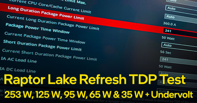
Thanks, that only really covers undervolting though as all results are 253W PL2 only or lower.
I can't remember where I saw it but somewhere plotted results out like this, all the way to 350W or so:
View attachment 334705


") I just give tips to friends and colleagues, and I always tell them to stay away from these money pits.
I just give tips to friends and colleagues, and I always tell them to stay away from these money pits.