
Well, given the fact that intel 10nm has the same density and characteristics, presumably, as the TSMC 7nm, then I think it is well deserved to do so. Samsung 5nm is also similar to TSMC 7nm, so everyone is trying to seem better then they actually are and funny enough, Intel is the most conservative right now with their naming. So stop being stupid and haters.
-
Welcome to TechPowerUp Forums, Guest! Please check out our forum guidelines for info related to our community.
You are using an out of date browser. It may not display this or other websites correctly.
You should upgrade or use an alternative browser.
You should upgrade or use an alternative browser.
Intel Could Rename its Semiconductor Nodes to Catch Up with the Industry
- Thread starter AleksandarK
- Start date

- Joined
- Nov 14, 2012
- Messages
- 1,693 (0.37/day)
| System Name | Meh |
|---|---|
| Processor | 7800X3D |
| Motherboard | MSI X670E Tomahawk |
| Cooling | Thermalright Phantom Spirit |
| Memory | 32GB G.Skill @ 6000/CL30 |
| Video Card(s) | Gainward RTX 4090 Phantom / Undervolt + OC |
| Storage | Samsung 990 Pro 2TB + WD SN850X 1TB + 64TB NAS/Server |
| Display(s) | 27" 1440p IPS @ 360 Hz + 32" 4K/UHD QD-OLED @ 240 Hz + 77" 4K/UHD QD-OLED @ 144 Hz VRR |
| Case | Fractal Design North XL |
| Audio Device(s) | FiiO DAC |
| Power Supply | Corsair RM1000x / Native 12VHPWR |
| Mouse | Logitech G Pro Wireless Superlight + Razer Deathadder V3 Pro |
| Keyboard | Corsair K60 Pro / MX Low Profile Speed |
| Software | Windows 10 Pro x64 |
There are actually people out there that do not requires the latest and fastest just for the sake of having it. I still have a old Phenom 2 x6 machine that I use daily, it does exactly what it needs to do and it does it solid as a rock after all these years.
If you can live with Ryzen 1600 performance, you might as well pick up an old Intel combo with BOARD, MEM and CPU for less than a new Ryzen 1600 and get identical performance if not better in gaming.
My old 2600K ran 5 GHz and easily beat Ryzen 1600 @ 4 GHz in 99.9% og games and applications
I'd never buy or recommend Ryzen 1000 series from NEW, probably not 2000 series either, unless it's cheap as dirt on sale, it's 3000 or 5000 series
1600AF is essentially 2600, only 1-2% slower (-200MHz base, -100MHz boost, same Zen+ die). And it seems like we have a bit different understanding of "not much more" for R5 3600. It's $130 vs $260, at least in my area. Basically you save half the price for 20-25% performance penalty. At that sub-$200 price range all you have is OEM R5 3500X, R3 3100/3300X which for some reason is always out of stock, or 3200G. 3500X is a cutdown version of 3600 with HT disabled, and while single-core performance is better, multi-core is within the margin of error comparing to 1600AF. And it's still more expensive.
Just because you don't buy it doesn't mean that the rest of the world doesn't.
Once again, I work with b2b sales and we have tons of huge retailers onboard, Ryzen 1000 is NOT selling like hotcakes, far from it.
What sells like hotcakes, especially in the laptop segment, is Intel, Intel and more Intel. Why? AMD can't deliver. Intel easily can, because they make their chips themself.
I think we ship 1 AMD laptop for every 100 Intel laptop, or so.
Irrelevant. We're talking about process nodes and not microarchitectures.
Irellevant, when someone with a Glofo 12nm calls Intel 14nm inferior? Yeah
 Suuuuuure.
TSMC is literally the reason why 3000 and especially 5000 performs great. If AMD were stuck with Glofo still, it would be a whole different story, with subpar clockspeeds like all 1000 and 2000 series chips.
Last edited:
- Joined
- Apr 10, 2020
- Messages
- 588 (0.31/day)
LOL... Rebranding will not make Intel's CPUs suck any less. There's only so much marketing department can do. Get your s***t together Intel, TSMC is rolling all over you.
- Joined
- Nov 20, 2013
- Messages
- 5,695 (1.34/day)
- Location
- Kyiv, Ukraine
| System Name | WS#1337 |
|---|---|
| Processor | Ryzen 7 5700X3D |
| Motherboard | ASUS X570-PLUS TUF Gaming |
| Cooling | Xigmatek Scylla 240mm AIO |
| Memory | 64GB DDR4-3600(4x16) |
| Video Card(s) | MSI RTX 3070 Gaming X Trio |
| Storage | ADATA Legend 2TB |
| Display(s) | Samsung Viewfinity Ultra S6 (34" UW) |
| Case | ghetto CM Cosmos RC-1000 |
| Audio Device(s) | ALC1220 |
| Power Supply | SeaSonic SSR-550FX (80+ GOLD) |
| Mouse | Logitech G603 |
| Keyboard | Modecom Volcano Blade (Kailh choc LP) |
| VR HMD | Google dreamview headset(aka fancy cardboard) |
| Software | Windows 11, Ubuntu 24.04 LTS |
It's still the case. Only 20 years ago we measured FET size as the smallest feature, and now it's fin or gate size, because on modern CPUs the term "transistor" became kinda vague.Well, to be honest, the last time that was true was I think 130nm. Since than, the "nm" is actually not the smallest feature, just a naming.
It gives manufacturers some leeway on what to pick as their metric and not end up being called a liar on technicalities )))
In which universe? Even if that were somehow true, it's a dead-end platform, so as anything up to Kaby Lake. Not only do you lose modern features, there's also no prospect for upgrade.My old 2600K ran 5 GHz and easily beat Ryzen 1600 @ 4 GHz in 99.9% og games and applications
And I'm Lisa Su's nephew.Once again, I work with b2b sales and we have tons of huge retailers onboard, Ryzen 1000 is NOT selling like hotcakes, far from it.
No need to retract to laptops. Let's keep going with overclocked 2600K that beats Zen+ in 99.9% of games and applications.What sells like hotcakes, especially in the laptop segment, is Intel
- Joined
- Oct 4, 2017
- Messages
- 719 (0.25/day)
- Location
- France
| Processor | RYZEN 7 5800X3D |
|---|---|
| Motherboard | Aorus B-550I Pro AX |
| Cooling | HEATKILLER IV PRO , EKWB Vector FTW3 3080/3090 , Barrow res + Xylem DDC 4.2, SE 240 + Dabel 20b 240 |
| Memory | Viper Steel 4000 PVS416G400C6K |
| Video Card(s) | EVGA 3080Ti FTW3 |
| Storage | XPG SX8200 Pro 512 GB NVMe + Samsung 980 1TB |
| Display(s) | ROG Strix OLED XG27AQDMG |
| Case | NR 200 |
| Power Supply | CORSAIR SF750 |
| Mouse | Logitech G PRO |
| Keyboard | Meletrix Zoom 75 GT Silver |
| Software | Windows 11 22H2 |
Renaming will not solve technical issues
Sure but this is not what Intel intended . Intels 10nm is very similar to TSMC 7nm physical size , same for their 7nm compared to TSMC 5nm ( if i recall correctly ) . This is what Intel intends to fix with this strategy .
Density isn't everything, in fact to get to such high clocks Intel had to sacrifice density on 14nm (with their ++ nodes) & IIRC even for ICL & TGL on 10nm. If you know about Si & how modern x86 designs have evolved you'll also know that "density" is in fact a huge issue for clocking the chips high (enough) & for desktops or HEDT it's not actually better!intel 10nm has the same density and characteristics, presumably, as the TSMC 7nm
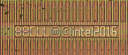
10NM CHANGES DIRECTION, TWICEIce Lake Rebadged to 10nm: Why?
So now we have Cannon Lake on ‘10nm’, and Ice Lake originally on 10+ but now rebadged to 10nm, but a different 10nm, with no real explanation as to why. In discussing with a number of peers and analysts in private conversations, the apparent conclusion they have come to is that Intel did not want to admit that its first generation of 10nm product had failed. Ever since then, Intel has attempted to quietly and discreetly shift Cannon Lake under the rug, as if it didn’t exist (it does exist, we did a big review on it, and Crimson Canyon is still for sale today at some of Intel’s biggest partners and major retailers).
Without Intel needing to admit that the first generation had failed, Ice Lake was the true ‘native’ 10nm product that was destined for life in the fast lane for consumers. If that was the case, then the low key presentation at CES 2018 stating it was shipping in 2017 was simply to meet investor targets. Intel never promoted Ice Lake as its first 10nm product, but the fact that the Cannon Lake product wasn't great meant that the company had to try and remove it from people's minds.
On Ice Lake, we studied the Ice Lake design, and we’ve seen lots of notebooks built on it. The fact that Intel called it ‘10th Gen’, and then also released the Comet Lake 14++++ product also called ‘10th Gen’, really ended up confusing the company even more, even in presentations to the press. It was the first time Intel had two products within the same generation of marketing name under different process nodes. It even confused OEM partner marketing teams as well as sales staff.
The problem with calling Ice Lake the new 10nm, is that internally the engineers still called it 10+. As Intel also announced other new products, such as Snow Ridge, or Lakefield, despite these meant to be called under the new 10nm, they would often be cited as ‘10+’ depending on which department of Intel you spoke to.
However, I now have an official decoder ring for you, to act as a reference for both users and Intel’s own engineers alike.
For clarity, 10nm Superfin is often abbreviated to 10SF, and 10nm Enhanced Superfin to 10ESF.
AnandTech's Decoder Ring for Intel's 10nm Product 2020+ First
UpdateOriginal Cannon Lake - - 10nm Ice Lake
Ice Lake-SP
Lakefield (compute)
Snow Ridge
Elkhart Lake10nm 10nm 10+ Tiger Lake
SG1
DG110nm
Superfin10+ 10++ Alder Lake
First Xe-HP GPU
Sapphire Rapids10nm
Enhanced
SuperFin10++ 10+++


Just to be clear, this is also for everyone who thinks that ICL is on the same 10nm as intended for CNL. It is not, ICL is the first 10nm+ product & probably wouldn't make it to the market if it was on the original 10nm node!
- Joined
- May 11, 2018
- Messages
- 1,661 (0.63/day)
Thank you, I haven't found the numbers I knew I read somewhere (estimations, there are no released specs).Zen2: 3.8 billion transistors on 74 mm² - 52 MTr/mm²
Zen3: 4.15 billion transistors on 80.6 mm² - 51.4 MTr/mm²
Renoir: 9.8 billion transistors on 156 mm² - 62.8 MTr/mm²
Intel transistors counts are really hard to come by. There was a throwaway comment in some financial call right after Ice Lake release saying it has over 7B transistors.
Ice Lake die that was the only one out at that point is 122.5 mm² which puts density at about 57 MTr/mm².
Same ballpark. Amount of different elements in the die (cache, GPU etc) probably play a bigger role in density of a specific chip at this point than manufacturing process.
Compared to the Intel promo material for 10nm it's quite a bit less dense:

- Joined
- Dec 26, 2006
- Messages
- 4,292 (0.63/day)
- Location
- Northern Ontario Canada
| Processor | Ryzen 5700x |
|---|---|
| Motherboard | Gigabyte X570S Aero G R1.1 Bios F7g |
| Cooling | Noctua NH-C12P SE14 w/ NF-A15 HS-PWM Fan 1500rpm |
| Memory | Micron DDR4-3200 2x32GB D.S. D.R. (CT2K32G4DFD832A) |
| Video Card(s) | AMD RX 6800 - Asus Tuf |
| Storage | Kingston KC3000 1TB & 2TB & 4TB Corsair MP600 Pro LPX |
| Display(s) | LG 27UL550-W (27" 4k) |
| Case | Be Quiet Pure Base 600 (no window) |
| Audio Device(s) | Realtek ALC1220-VB |
| Power Supply | SuperFlower Leadex V Gold Pro 850W ATX Ver2.52 |
| Mouse | Mionix Naos Pro |
| Keyboard | Corsair Strafe with browns |
| Software | W10 22H2 Pro x64 |
I can wait. I had a teacher long ago who use to say.............."don't wish your life away, it's already too short"Maybe they should. Because alot of fabs are too optimistic about their processnames.
GloFo 12nm was/is far worse than Intel 14nm for example.
Samsung 8nm is not great, but decent - Its probably worse than Intel 10nm
Intels 10nm, is more like TSMC 7nm.
I expect Intel 7nm will be more like TSMC 5nm or even 4nm.
If just performance and watt-usage is good, they can call it whatever they want, could not care less
The next few years are going to be interesting. Can't wait for next gen CPU platforms in 2022+ with DDR5 and PCIe 5.0, not going to get anything before DDR5 has matured (high clocks with decent timings - not going from top-end DDR4 to mediocre DDR5 on launch, thats for sure).

- Joined
- Apr 30, 2011
- Messages
- 2,786 (0.54/day)
- Location
- Greece
| Processor | AMD Ryzen 5 5600@80W |
|---|---|
| Motherboard | MSI B550 Tomahawk |
| Cooling | ZALMAN CNPS9X OPTIMA |
| Memory | 2*8GB PATRIOT PVS416G400C9K@3733MT_C16 |
| Video Card(s) | Sapphire Radeon RX 6750 XT Pulse 12GB |
| Storage | Sandisk SSD 128GB, Kingston A2000 NVMe 1TB, Samsung F1 1TB, WD Black 10TB |
| Display(s) | AOC 27G2U/BK IPS 144Hz |
| Case | SHARKOON M25-W 7.1 BLACK |
| Audio Device(s) | Realtek 7.1 onboard |
| Power Supply | Seasonic Core GC 500W |
| Mouse | Sharkoon SHARK Force Black |
| Keyboard | Trust GXT280 |
| Software | Win 7 Ultimate 64bit/Win 10 pro 64bit/Manjaro Linux |
Your CPU isn't a Phenom but a Thuban as all 6-core AMD CPUs back then, even if it was sold as a 4-core and you unlocked it.There are actually people out there that do not requires the latest and fastest just for the sake of having it. I still have a old Phenom 2 x6 machine that I use daily, it does exactly what it needs to do and it does it solid as a rock after all these years.
- Joined
- Sep 20, 2018
- Messages
- 1,463 (0.59/day)
i5 13400f, powered by Intels advanced ultra micro fine nanometer rising revengeance
- Joined
- Jan 14, 2019
- Messages
- 16,208 (6.82/day)
- Location
- Midlands, UK
| System Name | My second and third PCs are Intel + Nvidia |
|---|---|
| Processor | AMD Ryzen 7 7800X3D @ 45 W TDP Eco Mode |
| Motherboard | MSi Pro B650M-A Wifi |
| Cooling | Noctua NH-U9S chromax.black push+pull |
| Memory | 2x 24 GB Corsair Vengeance DDR5-6000 CL36 |
| Video Card(s) | PowerColor Reaper Radeon RX 9070 XT |
| Storage | 2 TB Corsair MP600 GS, 4 TB Seagate Barracuda |
| Display(s) | Dell S3422DWG 34" 1440 UW 144 Hz |
| Case | Corsair Crystal 280X |
| Audio Device(s) | Logitech Z333 2.1 speakers, AKG Y50 headphones |
| Power Supply | 750 W Seasonic Prime GX |
| Mouse | Logitech MX Master 2S |
| Keyboard | Logitech G413 SE |
| Software | Bazzite (Fedora Linux) KDE Plasma |
It must be really hard to figure out how many "+"-es to put at the end of node names. May I suggest firing all R&D staff, and employing more PR people to sort this out? They must really get it right for 12th gen.
- Joined
- Jan 8, 2017
- Messages
- 9,860 (3.17/day)
| System Name | Good enough |
|---|---|
| Processor | AMD Ryzen R9 7900 - Alphacool Eisblock XPX Aurora Edge |
| Motherboard | ASRock B650 Pro RS |
| Cooling | 2x 360mm NexXxoS ST30 X-Flow, 1x 360mm NexXxoS ST30, 1x 240mm NexXxoS ST30 |
| Memory | 32GB - FURY Beast RGB 5600 Mhz |
| Video Card(s) | Sapphire RX 7900 XT - Alphacool Eisblock Aurora |
| Storage | 1x Kingston KC3000 1TB 1x Kingston A2000 1TB, 1x Samsung 850 EVO 250GB , 1x Samsung 860 EVO 500GB |
| Display(s) | LG UltraGear 32GN650-B + 4K Samsung TV |
| Case | Phanteks NV7 |
| Power Supply | GPS-750C |
I am pretty sure that's what they've been doing all along.May I suggest firing all R&D staff, and employing more PR people to sort this out?

- Joined
- Dec 29, 2010
- Messages
- 3,926 (0.74/day)
| Processor | AMD 5900x |
|---|---|
| Motherboard | Asus x570 Strix-E |
| Cooling | Hardware Labs |
| Memory | G.Skill 4000c17 2x16gb |
| Video Card(s) | RTX 3090 |
| Storage | Sabrent |
| Display(s) | Samsung G9 |
| Case | Phanteks 719 |
| Audio Device(s) | Fiio K5 Pro |
| Power Supply | EVGA 1000 P2 |
| Mouse | Logitech G600 |
| Keyboard | Corsair K95 |
Haha! That's brilliant! Just lie and call it whatever you want. Then again this is the company that uses waterchillers hidden under tables to lie about their great new cpus.

- Joined
- Mar 10, 2010
- Messages
- 11,880 (2.12/day)
- Location
- Manchester uk
| System Name | RyzenGtEvo/ Asus strix scar II |
|---|---|
| Processor | Amd R5 5900X/ Intel 8750H |
| Motherboard | Crosshair hero8 impact/Asus |
| Cooling | 360EK extreme rad+ 360$EK slim all push, cpu ek suprim Gpu full cover all EK |
| Memory | Gskill Trident Z 3900cas18 32Gb in four sticks./16Gb/16GB |
| Video Card(s) | Asus tuf RX7900XT /Rtx 2060 |
| Storage | Silicon power 2TB nvme/8Tb external/1Tb samsung Evo nvme 2Tb sata ssd/1Tb nvme |
| Display(s) | Samsung UAE28"850R 4k freesync.dell shiter |
| Case | Lianli 011 dynamic/strix scar2 |
| Audio Device(s) | Xfi creative 7.1 on board ,Yamaha dts av setup, corsair void pro headset |
| Power Supply | corsair 1200Hxi/Asus stock |
| Mouse | Roccat Kova/ Logitech G wireless |
| Keyboard | Roccat Aimo 120 |
| VR HMD | Oculus rift |
| Software | Win 10 Pro |
| Benchmark Scores | laptop Timespy 6506 |
To be fair Intel did try to introduce common sense metrics to quantify nodes but no one else bit, clearly, if you can't beat em join em.
Hopefully Alderlake or nextlake shake's things up.
Hopefully Alderlake or nextlake shake's things up.
- Joined
- Aug 20, 2007
- Messages
- 22,551 (3.45/day)
- Location
- Olympia, WA
| System Name | Pioneer |
|---|---|
| Processor | Ryzen 9 9950X |
| Motherboard | MSI MAG X670E Tomahawk Wifi |
| Cooling | Noctua NH-D15 + A whole lotta Sunon, Phanteks and Corsair Maglev blower fans... |
| Memory | 64GB (2x 32GB) G.Skill Flare X5 @ DDR5-6200(Running 1T no GDM) |
| Video Card(s) | PNY RTX 5080 OC |
| Storage | Intel 5800X Optane 800GB boot, +2x Crucial P5 Plus 2TB PCIe 4.0 NVMe SSDs, 1x 2TB Seagate Exos 3.5" |
| Display(s) | 55" Hisense 55U8N 4K FALD Display |
| Case | Thermaltake Core X31 |
| Audio Device(s) | TOSLINK->Schiit Modi MB->Asgard 2 DAC Amp->AKG Pro K712 Headphones or HDMI->B9 OLED |
| Power Supply | FSP Hydro Ti Pro 850W 80Plus Titanium PSU |
| Mouse | Logitech G305 Lightspeed Wireless |
| Keyboard | WASD Code v3 with Cherry Green keyswitches + PBT DS keycaps |
| Software | Gentoo Linux x64 / Windows 11 Enterprise (yes it's legit) |
This. Basically intel was the only one using common sense node metrics, and it made them sound way more behind than they were (dont get me wrong, they ARE behind, but everyone else is making up numbers that really don't match reality so it's pretty much only fair intel finally can do the same).To be fair Intel did try to introduce common sense metrics to quantify nodes but no one else bit, clearly, if you can't beat em join em.
Hopefully Alderlake or nextlake shake's things up.
Well there was a calculation done on Intel's 10nm logic to be 100Mtr/mm^2 where the wikichips is based off, obviously thats only the densest part and not the entirety.
 hexus.net
Intel 10nm density is 2.7X improved over its 14nm node
New report says that Intel can pack 100.8 million transistors per square mm.
hexus.net
Last edited:
- Joined
- Jan 31, 2011
- Messages
- 2,237 (0.42/day)
| System Name | Ultima |
|---|---|
| Processor | AMD Ryzen 7 5800X |
| Motherboard | MSI Mag B550M Mortar |
| Cooling | Arctic Liquid Freezer II 240 rev4 w/ Ryzen offset mount |
| Memory | G.SKill Ripjaws V 2x16GB DDR4 3600 |
| Video Card(s) | Palit GeForce RTX 4070 12GB Dual |
| Storage | WD Black SN850X 2TB Gen4, Samsung 970 Evo Plus 500GB , 1TB Crucial MX500 SSD sata, |
| Display(s) | ASUS TUF VG249Q3A 24" 1080p 165-180Hz VRR |
| Case | DarkFlash DLM21 Mesh |
| Audio Device(s) | Onboard Realtek ALC1200 Audio/Nvidia HD Audio |
| Power Supply | Corsair RM650 |
| Mouse | Rog Strix Impact 3 Wireless | Wacom Intuos CTH-480 |
| Keyboard | A4Tech B314 Keyboard |
| Software | Windows 10 Pro |
Did you post this article a day early?
- Joined
- Feb 23, 2008
- Messages
- 1,094 (0.17/day)
- Location
- Montreal
| System Name | Aryzen / Sairikiki / Tesseract |
|---|---|
| Processor | 5800x / i7 920@3.73 / 5800x |
| Motherboard | Steel Legend B450M / GB EX58-UDP4 / Steel Legend B550M |
| Cooling | Mugen 5 / Pure Rock / Glacier One 240 |
| Memory | Corsair Something 16 / Corsair Something 12 / G.Skill 32 |
| Video Card(s) | AMD 6800XT / AMD 6750XT / Sapphire 7800XT |
| Storage | Way too many drives... |
| Display(s) | LG 332GP850-B / Sony w800b / Sony X90J |
| Case | EVOLV X / Carbide 540 / Carbide 280x |
| Audio Device(s) | SB ZxR + GSP 500 / board / Denon X1700h + ELAC Uni-Fi 2 + Senn 6XX |
| Power Supply | Seasonic PRIME GX-750 / Corsair HX750 / Seasonic Focus PX-650 |
| Mouse | G700 / none / G602 |
| Keyboard | G910 |
| Software | w11 64 |
| Benchmark Scores | I don't play benchmarks... |
I guess that's one way to "catch up"...
To be honest, they can name their nodes whatever they want. At the end of the day, people will just look at the density and efficiency of the node. For example, you can have a supposed 5nm, but actually fare no better than a 7nm, that will become apparent in product reviews. Right now, TSMC is leading and thus, not much to compare. If Intel joins the party late, it will be easier to scrutinize.
- Joined
- Feb 3, 2017
- Messages
- 4,022 (1.30/day)
| Processor | Ryzen 7800X3D |
|---|---|
| Motherboard | ROG STRIX B650E-F GAMING WIFI |
| Memory | 2x16GB G.Skill Flare X5 DDR5-6000 CL36 (F5-6000J3636F16GX2-FX5) |
| Video Card(s) | INNO3D GeForce RTX™ 4070 Ti SUPER TWIN X2 |
| Storage | 2TB Samsung 980 PRO, 4TB WD Black SN850X |
| Display(s) | 42" LG C2 OLED, 27" ASUS PG279Q |
| Case | Thermaltake Core P5 |
| Power Supply | Fractal Design Ion+ Platinum 760W |
| Mouse | Corsair Dark Core RGB Pro SE |
| Keyboard | Corsair K100 RGB |
| VR HMD | HTC Vive Cosmos |
The marketable numbers are always with the densest variant of the process node. Practically every manufacturing process has separate variants targeted towards density and performance. Performance variant usually has about 1/3 less transistors on the same area. The basic idea is more empty space between cells/transistors to allow higher voltages with lower leakage.Thank you, I haven't found the numbers I knew I read somewhere (estimations, there are no released specs).
Compared to the Intel promo material for 10nm it's quite a bit less dense:
High Density variant is canonically used for mobile and other dies aiming at low power (and lower frequencies), High Performance variant are used - as the name says - high performance dies running at higher voltages, higher frequencies and higher power consumption.
Anandtech's 10nm Cannon Lake article laid out the Intel 10nm spec, scroll down to 'There's more to it' section - 100 MTr/mm² for High Density, 67 MTr/mm² for Ultra High Performance:
Intel's 10nm Cannon Lake and Core i3-8121U Deep Dive Review
All the official numbers are standard cells - or something more dense like SRAM if manufacturer wants to show even larger density numbers. The actual dies (like CPUs or GPUs) are usually less dense than that due to number of reasons. Logic circuitry does not lend well to being tightly packed together, there are areas like IO that do not scale down that well etc.