- Joined
- Oct 9, 2007
- Messages
- 47,680 (7.42/day)
- Location
- Dublin, Ireland
| System Name | RBMK-1000 |
|---|---|
| Processor | AMD Ryzen 7 5700G |
| Motherboard | Gigabyte B550 AORUS Elite V2 |
| Cooling | DeepCool Gammax L240 V2 |
| Memory | 2x 16GB DDR4-3200 |
| Video Card(s) | Galax RTX 4070 Ti EX |
| Storage | Samsung 990 1TB |
| Display(s) | BenQ 1440p 60 Hz 27-inch |
| Case | Corsair Carbide 100R |
| Audio Device(s) | ASUS SupremeFX S1220A |
| Power Supply | Cooler Master MWE Gold 650W |
| Mouse | ASUS ROG Strix Impact |
| Keyboard | Gamdias Hermes E2 |
| Software | Windows 11 Pro |
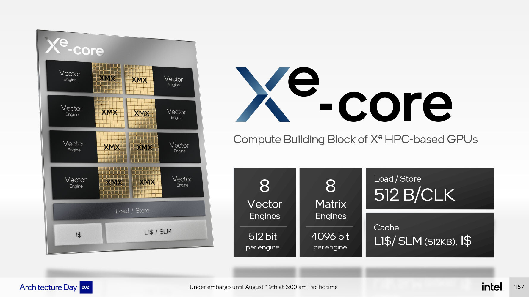
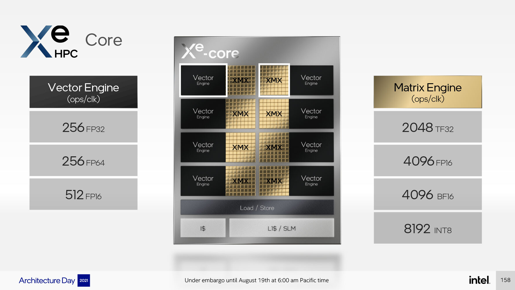
Intel's Xe HPC (high performance compute) architecture powers the company's most powerful vector compute device to date, codenamed "Ponte Vecchio." The processor is designed for massive HPC and AI compute applications, but also features raster graphics and real-time raytracing hardware, giving it a dual-use as a cloud gaming GPU. Our Xe HPG architecture article covers the basics of how Intel is laying its client discrete GPUs out. The Xe HPC architecture both scales-up and scales-out from that. The Xe-core, the basic indivisible sub-unit, of the Xe HPC architecture is different from that of Xe HPG. While Xe HPG cores contain sixteen 256-bit vector engines alongside sixteen 1024-bit matrix engines; the Xe HPC cores features eight 512-bit vector engines, besides eight 4096-bit matrix engines. It also features higher load/store throughput, and a larger 512 KB L1 cache.


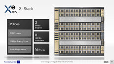
The Xe HPC core vector unit is designed for full FP64 performance, of 256 ops per clock, which is identical to its FP32 throughput. It also offers 512 ops/clock FP16. The matrix unit, on the other hand, packs a punch—2,048 TF32 ops/cycle, up to 4,096 FP16 and BFloat16 ops/cycle, and 8,192 INT8 ops/cycle. Things get interesting as we scale up from here. The Xe HPC Slice is a grouping of 16 Xe HPC cores, along with 16 dedicated Raytracing Units that are just as capable as the ones on the Xe HPG (calculating ray traversal, bounding box intersection, and triangle intersection). The Xe HPC Slice cumulatively has 8 MB of L1 cache on its own.


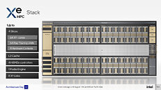
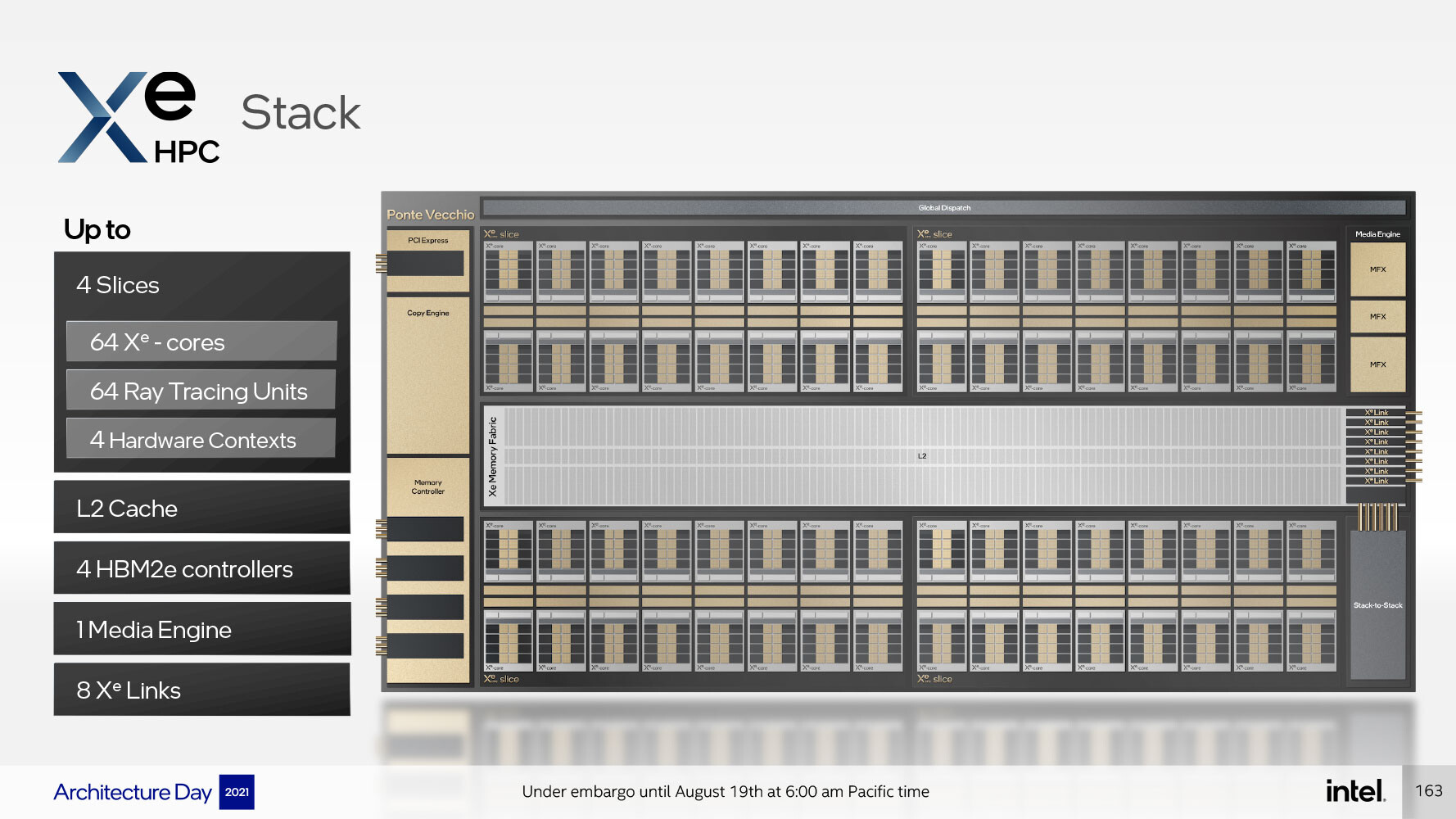
A Xe HPC compute tile, or Xe HPC Stack, contains four such Xe HPC Slices, 64 Xe HPC cores, 64 Raytracing Units, 4 hardware contexts, sharing a large 144 MB L2 cache. The uncore components include a PCI-Express 5.0 x16 interface, a 4096-bit wide HBM2E memory interface, a media-acceleration engine with fixed-function hardware to accelerate decode (and possibly encode) of popular video formats, and Xe Link, an interconnect designed to interface with up to 8 other Xe HPC dual-stacks, for a total of up to 16 stacks. Each dual-stack uses a low-latency stack-to-stack interconnect. A dual-stack hence ends up to 128 Xe HPC cores, 128 Raytracing Units, two media engines, and an 8192-bit wide HBM2E interface. The dual-stack is a relevant grouping here, as the "Ponte Vecchio" processor features two compute tiles (two Xe HPG Stacks), and eight HBM2E memory stacks.


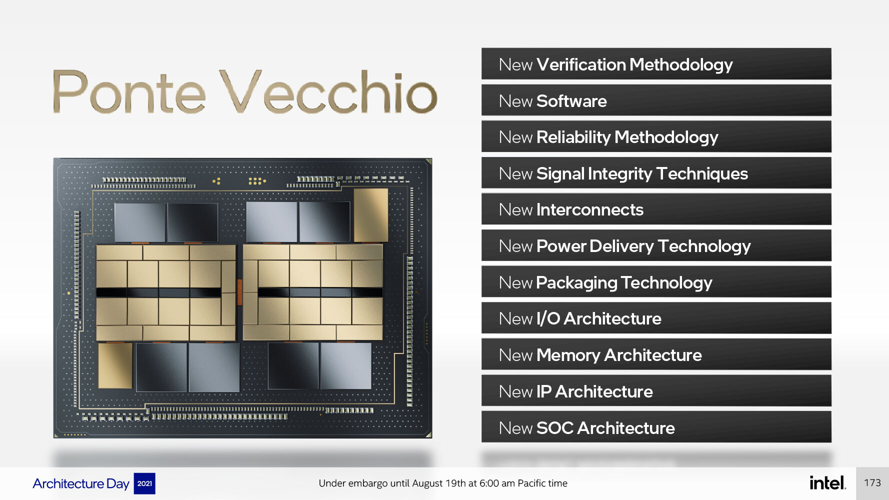
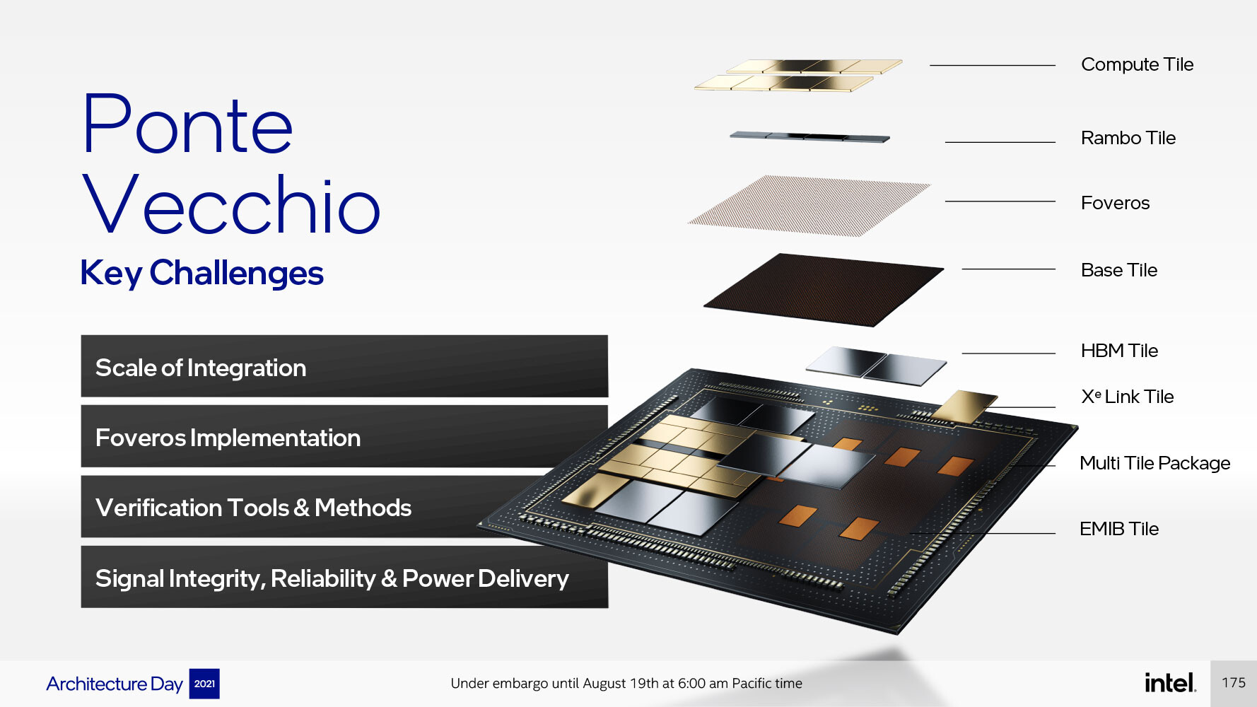
It's important to note here, that the Xe HPC Slices sit in specialized dies called compute tiles that are fabricated TSMC's 5 nm N5 node, whie the rest of the hardware sits on a base die that's built on the Intel 7 node (10 nm Enhanced SuperFin). The two dies are Foveros-stacked with 36-micron bumps. The Xe Link tile is a separate piece of silicon dedicated for networking with neighboring packages. This die is built on TSMC 7 nm node, and consists mainly of SerDes (serializer-deserializer) components.


Each "Ponte Vecchio" OAM with two Xe HPC stacks (one MCM) a combined memory bandwidth of over 5 TB/s, and Xe Link connectivity bandwidth of over 2 TB/s. A "Ponte Vecchio" x4 Subsystem holds four such OAMs, and is designed for a 1U node with two Xeon "Sapphire Rapids" processors. The four "Ponte Vecchio" and two "Sapphire Rapids" packages are each liquid-cooled. Hardware is only part of the story, Intel is investing considerably on OneAPI, a collective programming environment for both the CPU and GPU.


View at TechPowerUp Main Site

The Xe HPC core vector unit is designed for full FP64 performance, of 256 ops per clock, which is identical to its FP32 throughput. It also offers 512 ops/clock FP16. The matrix unit, on the other hand, packs a punch—2,048 TF32 ops/cycle, up to 4,096 FP16 and BFloat16 ops/cycle, and 8,192 INT8 ops/cycle. Things get interesting as we scale up from here. The Xe HPC Slice is a grouping of 16 Xe HPC cores, along with 16 dedicated Raytracing Units that are just as capable as the ones on the Xe HPG (calculating ray traversal, bounding box intersection, and triangle intersection). The Xe HPC Slice cumulatively has 8 MB of L1 cache on its own.
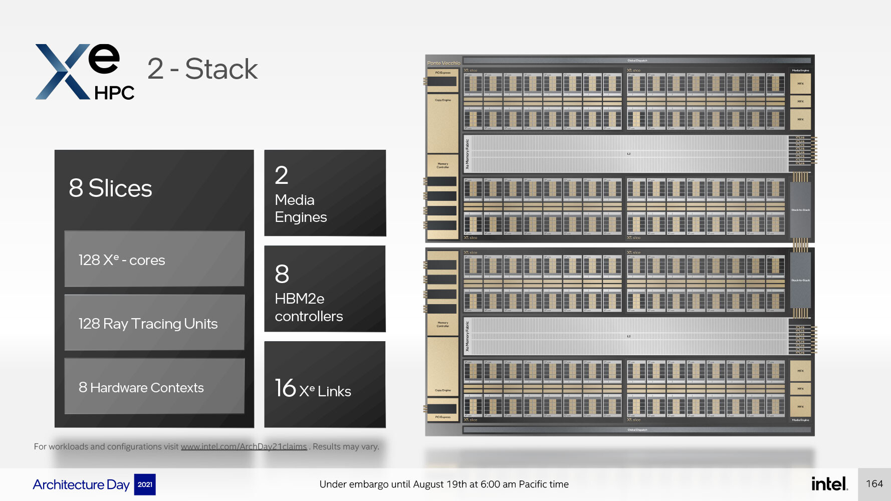


A Xe HPC compute tile, or Xe HPC Stack, contains four such Xe HPC Slices, 64 Xe HPC cores, 64 Raytracing Units, 4 hardware contexts, sharing a large 144 MB L2 cache. The uncore components include a PCI-Express 5.0 x16 interface, a 4096-bit wide HBM2E memory interface, a media-acceleration engine with fixed-function hardware to accelerate decode (and possibly encode) of popular video formats, and Xe Link, an interconnect designed to interface with up to 8 other Xe HPC dual-stacks, for a total of up to 16 stacks. Each dual-stack uses a low-latency stack-to-stack interconnect. A dual-stack hence ends up to 128 Xe HPC cores, 128 Raytracing Units, two media engines, and an 8192-bit wide HBM2E interface. The dual-stack is a relevant grouping here, as the "Ponte Vecchio" processor features two compute tiles (two Xe HPG Stacks), and eight HBM2E memory stacks.


It's important to note here, that the Xe HPC Slices sit in specialized dies called compute tiles that are fabricated TSMC's 5 nm N5 node, whie the rest of the hardware sits on a base die that's built on the Intel 7 node (10 nm Enhanced SuperFin). The two dies are Foveros-stacked with 36-micron bumps. The Xe Link tile is a separate piece of silicon dedicated for networking with neighboring packages. This die is built on TSMC 7 nm node, and consists mainly of SerDes (serializer-deserializer) components.


Each "Ponte Vecchio" OAM with two Xe HPC stacks (one MCM) a combined memory bandwidth of over 5 TB/s, and Xe Link connectivity bandwidth of over 2 TB/s. A "Ponte Vecchio" x4 Subsystem holds four such OAMs, and is designed for a 1U node with two Xeon "Sapphire Rapids" processors. The four "Ponte Vecchio" and two "Sapphire Rapids" packages are each liquid-cooled. Hardware is only part of the story, Intel is investing considerably on OneAPI, a collective programming environment for both the CPU and GPU.


View at TechPowerUp Main Site


") ) to implement?
) to implement?