-
Welcome to TechPowerUp Forums, Guest! Please check out our forum guidelines for info related to our community.
You are using an out of date browser. It may not display this or other websites correctly.
You should upgrade or use an alternative browser.
You should upgrade or use an alternative browser.
NVIDIA GV102 Prototype Board With GDDR6 Spotted, Up to 525 W Power Delivery. GTX 1180 Ti?
- Thread starter W1zzard
- Start date


- Joined
- Mar 14, 2008
- Messages
- 511 (0.08/day)
- Location
- DK
| System Name | Main setup |
|---|---|
| Processor | i9 12900K |
| Motherboard | Gigabyte z690 Gaming X |
| Cooling | Water |
| Memory | Kingston 32GB 5200@cl30 |
| Video Card(s) | Asus Tuf RTS 4090 |
| Storage | Adata SX8200 PRO 1 adn 2 TB, Samsung 960EVO, Crucial MX300 750GB Limited edition |
| Display(s) | HP "cheapass" 34" 3440x1440 |
| Case | CM H500P Mesh |
| Audio Device(s) | Logitech G933 |
| Power Supply | Corsair RX850i |
| Mouse | G502 |
| Keyboard | SteelSeries Apex Pro |
| Software | W11 |
Maybe they are doing an intel…… LOOK AT THIS CART running 5Ghz...… 
- Joined
- Jun 10, 2014
- Messages
- 3,128 (0.77/day)
| Processor | AMD Ryzen 9 5900X ||| Intel Core i7-3930K |
|---|---|
| Motherboard | ASUS ProArt B550-CREATOR ||| Asus P9X79 WS |
| Cooling | Noctua NH-U14S ||| Be Quiet Pure Rock |
| Memory | Crucial 2 x 16 GB 3200 MHz ||| Corsair 8 x 8 GB 1333 MHz |
| Video Card(s) | MSI GTX 1060 3GB ||| MSI GTX 680 4GB |
| Storage | Samsung 970 PRO 512 GB + 1 TB ||| Intel 545s 512 GB + 256 GB |
| Display(s) | Asus ROG Swift PG278QR 27" ||| Eizo EV2416W 24" |
| Case | Fractal Design Define 7 XL x 2 |
| Audio Device(s) | Cambridge Audio DacMagic Plus |
| Power Supply | Seasonic Focus PX-850 x 2 |
| Mouse | Razer Abyssus |
| Keyboard | CM Storm QuickFire XT |
| Software | Ubuntu |
I know there was some talk of bringing NVLink to GeForce products a long time ago, but I haven't heard anything lately. NVLink on a prototype board does not mean consumer products will feature it, but at least it indicates "GV102" supports it. I do wonder why they have rotated it vs. other boards.
- Joined
- May 22, 2015
- Messages
- 14,413 (3.89/day)
| Processor | Intel i5-12600k |
|---|---|
| Motherboard | Asus H670 TUF |
| Cooling | Arctic Freezer 34 |
| Memory | 2x16GB DDR4 3600 G.Skill Ripjaws V |
| Video Card(s) | EVGA GTX 1060 SC |
| Storage | 500GB Samsung 970 EVO, 500GB Samsung 850 EVO, 1TB Crucial MX300 and 2TB Crucial MX500 |
| Display(s) | Dell U3219Q + HP ZR24w |
| Case | Raijintek Thetis |
| Audio Device(s) | Audioquest Dragonfly Red :D |
| Power Supply | Seasonic 620W M12 |
| Mouse | Logitech G502 Proteus Core |
| Keyboard | G.Skill KM780R |
| Software | Arch Linux + Win10 |
NVLink could be needed when the data being shuffled around increases past a certain limit. But I don't think we're there just yet.I know there was some talk of bringing NVLink to GeForce products a long time ago, but I haven't heard anything lately. NVLink on a prototype board does not mean consumer products will feature it, but at least it indicates "GV102" supports it. I do wonder why they have rotated it vs. other boards.
- Joined
- May 7, 2012
- Messages
- 2,597 (0.54/day)
- Location
- Rhode Island
| System Name | Whaaaat Kiiiiiiid! |
|---|---|
| Processor | Intel Core i9-14900K @ Default |
| Motherboard | Gigabyte Z690 AORUS Elite AX DDR4 |
| Cooling | Corsair H150i AIO Cooler |
| Memory | Corsair Dominator Platinum 128GB DDR4-3200 |
| Video Card(s) | EVGA GeForce RTX 3080 FTW3 ULTRA @ Default |
| Storage | Samsung 970 PRO 512GB + Crucial MX500 2TB x3 + Crucial MX500 4TB + Samsung 980 PRO 1TB |
| Display(s) | 27" LG 27MU67-B 4K, + 27" Acer Predator XB271HU 1440P |
| Case | Thermaltake Core X9 Snow |
| Audio Device(s) | Logitech G PRO X 2 Lightspeed |
| Power Supply | SeaSonic Platinum 1050W Snow Silent |
| Mouse | Logitech G903 Lightspeed |
| Keyboard | Logitech G915 X Lightspeed |
| Software | Windows 11 Pro |
| Benchmark Scores | FFXV: 19329 |
since GV100 (5376 cuda cores) when all SMs are unlocked a new Titan Xv could be 5376
Last edited:

- Joined
- Jul 18, 2012
- Messages
- 531 (0.11/day)
- Location
- Germany
| Processor | R7 5700x |
|---|---|
| Motherboard | MSI B450i Gaming |
| Cooling | Accelero Mono CPU Edition |
| Memory | 16 GB VLP |
| Video Card(s) | RX 7900 GRE Dual |
| Storage | P34A80 512GB |
| Display(s) | LG 27UM67 UHD |
| Case | none |
| Power Supply | Fractal Ion 650 SFX |
It's only a little bigger as GP102 so it's either a small Volta, which I find unlikely, or the big Turing with ~ 72 SMs.

- Joined
- May 7, 2012
- Messages
- 2,597 (0.54/day)
- Location
- Rhode Island
| System Name | Whaaaat Kiiiiiiid! |
|---|---|
| Processor | Intel Core i9-14900K @ Default |
| Motherboard | Gigabyte Z690 AORUS Elite AX DDR4 |
| Cooling | Corsair H150i AIO Cooler |
| Memory | Corsair Dominator Platinum 128GB DDR4-3200 |
| Video Card(s) | EVGA GeForce RTX 3080 FTW3 ULTRA @ Default |
| Storage | Samsung 970 PRO 512GB + Crucial MX500 2TB x3 + Crucial MX500 4TB + Samsung 980 PRO 1TB |
| Display(s) | 27" LG 27MU67-B 4K, + 27" Acer Predator XB271HU 1440P |
| Case | Thermaltake Core X9 Snow |
| Audio Device(s) | Logitech G PRO X 2 Lightspeed |
| Power Supply | SeaSonic Platinum 1050W Snow Silent |
| Mouse | Logitech G903 Lightspeed |
| Keyboard | Logitech G915 X Lightspeed |
| Software | Windows 11 Pro |
| Benchmark Scores | FFXV: 19329 |
Its most likely a smaller volta like 102 pascal was to 100 with same core countIt's only a little bigger as GP102 so it's either a small Volta, which I find unlikely, or the big Turing with ~ 72 SMs.
View attachment 103138
610 gp100
470 gp102 same core count
So 800 to 600 is plausable 5120 each
D
Deleted member 177333
Guest
If they made a new kickass SLI connector that fixes the downfalls I would love to buy 2
Ya, I keep seeing people note that developers, etc. want to eliminate multi-gpu...that would be kinda crappy for some gamers. I mean right now the only way I am able to play a # of my newer games in 4k / 60fps is because of SLI. Without SLI, most folks would be stuck in the 1440p / 1080p resolutions still if they want to play with excellent framerates. So I am hopeful that you're right and it's just maybe a newer connector with more bandwidth, etc.
- Joined
- May 22, 2015
- Messages
- 14,413 (3.89/day)
| Processor | Intel i5-12600k |
|---|---|
| Motherboard | Asus H670 TUF |
| Cooling | Arctic Freezer 34 |
| Memory | 2x16GB DDR4 3600 G.Skill Ripjaws V |
| Video Card(s) | EVGA GTX 1060 SC |
| Storage | 500GB Samsung 970 EVO, 500GB Samsung 850 EVO, 1TB Crucial MX300 and 2TB Crucial MX500 |
| Display(s) | Dell U3219Q + HP ZR24w |
| Case | Raijintek Thetis |
| Audio Device(s) | Audioquest Dragonfly Red :D |
| Power Supply | Seasonic 620W M12 |
| Mouse | Logitech G502 Proteus Core |
| Keyboard | G.Skill KM780R |
| Software | Arch Linux + Win10 |
I guess SLi/Crossfire's death is not because they're completely useless, but because the ROI is not there. Too few people use that feature.Ya, I keep seeing people note that developers, etc. want to eliminate multi-gpu...that would be kinda crappy for some gamers. I mean right now the only way I am able to play a # of my newer games in 4k / 60fps is because of SLI. Without SLI, most folks would be stuck in the 1440p / 1080p resolutions still if they want to play with excellent framerates. So I am hopeful that you're right and it's just maybe a newer connector with more bandwidth, etc.
- Joined
- Mar 14, 2014
- Messages
- 1,518 (0.37/day)
| Processor | 11900K |
|---|---|
| Motherboard | ASRock Z590 OC Formula |
| Cooling | Noctua NH-D15 using 2x140mm 3000RPM industrial Noctuas |
| Memory | G. Skill Trident Z 2x16GB 3600MHz |
| Video Card(s) | eVGA RTX 3090 FTW3 |
| Storage | 2TB Crucial P5 Plus |
| Display(s) | 1st: LG GR83Q-B 1440p 27in 240Hz / 2nd: Lenovo y27g 1080p 27in 144Hz |
| Case | Lian Li Lancool MESH II RGB (I removed the RGB) |
| Audio Device(s) | AKG Q701's w/ O2+ODAC (Sounds a little bright) |
| Power Supply | Seasonic Prime 850 TX |
| Mouse | Glorious Model D |
| Keyboard | Glorious MMK2 65% Lynx MX switches |
| Software | Win10 Pro |
Yeah I don't really see multi-gpu dying..Nivida loves to sell extra cards they won't let it die.Ya, I keep seeing people note that developers, etc. want to eliminate multi-gpu...that would be kinda crappy for some gamers. I mean right now the only way I am able to play a # of my newer games in 4k / 60fps is because of SLI. Without SLI, most folks would be stuck in the 1440p / 1080p resolutions still if they want to play with excellent framerates. So I am hopeful that you're right and it's just maybe a newer connector with more bandwidth, etc.
- Joined
- Jun 10, 2014
- Messages
- 3,128 (0.77/day)
| Processor | AMD Ryzen 9 5900X ||| Intel Core i7-3930K |
|---|---|
| Motherboard | ASUS ProArt B550-CREATOR ||| Asus P9X79 WS |
| Cooling | Noctua NH-U14S ||| Be Quiet Pure Rock |
| Memory | Crucial 2 x 16 GB 3200 MHz ||| Corsair 8 x 8 GB 1333 MHz |
| Video Card(s) | MSI GTX 1060 3GB ||| MSI GTX 680 4GB |
| Storage | Samsung 970 PRO 512 GB + 1 TB ||| Intel 545s 512 GB + 256 GB |
| Display(s) | Asus ROG Swift PG278QR 27" ||| Eizo EV2416W 24" |
| Case | Fractal Design Define 7 XL x 2 |
| Audio Device(s) | Cambridge Audio DacMagic Plus |
| Power Supply | Seasonic Focus PX-850 x 2 |
| Mouse | Razer Abyssus |
| Keyboard | CM Storm QuickFire XT |
| Software | Ubuntu |
GV100 and GV102 will have 6 GPCs, 84 SMs and 5376 Cuda cores.It's only a little bigger as GP102 so it's either a small Volta, which I find unlikely, or the big Turing with ~ 72 SMs.
GV104 will have 4 GPCs, 56 SMs, and 3584 Cuda cores.
GV106 will have 2 GPCs, 28 SMs, and 1792 Cuda cores.
GV102 will have fewer fp64 units, but we don't yet know if the tensor unit count is the same.
- Joined
- Jul 18, 2012
- Messages
- 531 (0.11/day)
- Location
- Germany
| Processor | R7 5700x |
|---|---|
| Motherboard | MSI B450i Gaming |
| Cooling | Accelero Mono CPU Edition |
| Memory | 16 GB VLP |
| Video Card(s) | RX 7900 GRE Dual |
| Storage | P34A80 512GB |
| Display(s) | LG 27UM67 UHD |
| Case | none |
| Power Supply | Fractal Ion 650 SFX |
IMO, Volta was a pure AI/HPC oriented GPU so I doubt we'll see it ever in mainstream consumer cards. They might have a GV102, just like you said but not the rest. That will be based on Volta_v2/Turing.GV100 and GV102 will have 6 GPCs, 84 SMs and 5376 Cuda cores.
GV104 will have 4 GPCs, 56 SMs, and 3584 Cuda cores.
GV106 will have 2 GPCs, 28 SMs, and 1792 Cuda cores.
GV102 will have fewer fp64 units, but we don't yet know if the tensor unit count is the same.
TSMCs 12nm process offers about 20% higher density.. They would have to go beyond 400mm² for 40% cores, something they haven't done for their high end chips.
Last edited:
- Joined
- May 22, 2015
- Messages
- 14,413 (3.89/day)
| Processor | Intel i5-12600k |
|---|---|
| Motherboard | Asus H670 TUF |
| Cooling | Arctic Freezer 34 |
| Memory | 2x16GB DDR4 3600 G.Skill Ripjaws V |
| Video Card(s) | EVGA GTX 1060 SC |
| Storage | 500GB Samsung 970 EVO, 500GB Samsung 850 EVO, 1TB Crucial MX300 and 2TB Crucial MX500 |
| Display(s) | Dell U3219Q + HP ZR24w |
| Case | Raijintek Thetis |
| Audio Device(s) | Audioquest Dragonfly Red :D |
| Power Supply | Seasonic 620W M12 |
| Mouse | Logitech G502 Proteus Core |
| Keyboard | G.Skill KM780R |
| Software | Arch Linux + Win10 |
Oh it's dying, make no mistake. Support has already been moved from the drivers to DX12 and Vulkan and pretty much no developer cared enough to pick up the slack.Yeah I don't really see multi-gpu dying..
Considering multi GPU is run by less than 1% of the users (and not all of them are running Nvidia), I'd be really surprised if extra income from that segment actually registered on Nvidia's radar.Nivida loves to sell extra cards they won't let it die.
- Joined
- Jun 10, 2014
- Messages
- 3,128 (0.77/day)
| Processor | AMD Ryzen 9 5900X ||| Intel Core i7-3930K |
|---|---|
| Motherboard | ASUS ProArt B550-CREATOR ||| Asus P9X79 WS |
| Cooling | Noctua NH-U14S ||| Be Quiet Pure Rock |
| Memory | Crucial 2 x 16 GB 3200 MHz ||| Corsair 8 x 8 GB 1333 MHz |
| Video Card(s) | MSI GTX 1060 3GB ||| MSI GTX 680 4GB |
| Storage | Samsung 970 PRO 512 GB + 1 TB ||| Intel 545s 512 GB + 256 GB |
| Display(s) | Asus ROG Swift PG278QR 27" ||| Eizo EV2416W 24" |
| Case | Fractal Design Define 7 XL x 2 |
| Audio Device(s) | Cambridge Audio DacMagic Plus |
| Power Supply | Seasonic Focus PX-850 x 2 |
| Mouse | Razer Abyssus |
| Keyboard | CM Storm QuickFire XT |
| Software | Ubuntu |
It will feature the resources needed for raytracing through Nvidia's "RTX technology", which Pascal lacks. But GV102 might not have the same amount of tensor cores as GV100.IMO, Volta was a pure AI/HPC oriented GPU so I doubt we'll see it ever in mainstream consumer cards. They might have a GV102, just like you said but not the rest. That will be based on Volta_v2/Turing.
TSMCs 12nm process offers about 20% higher density.. They would have to go beyond 400mm², something they haven't done for their high end chips.
Where do you get that TSMC's "12 nm" is 20% denser? GV100 is not denser, and TSMC "12 nm" is still the same node just with improved thermals. Pascal is not pushing the maximum density of TSMC's "16 nm". Expect the density of GV102/GV104 to be in the same range as before.
- Joined
- Jul 18, 2012
- Messages
- 531 (0.11/day)
- Location
- Germany
| Processor | R7 5700x |
|---|---|
| Motherboard | MSI B450i Gaming |
| Cooling | Accelero Mono CPU Edition |
| Memory | 16 GB VLP |
| Video Card(s) | RX 7900 GRE Dual |
| Storage | P34A80 512GB |
| Display(s) | LG 27UM67 UHD |
| Case | none |
| Power Supply | Fractal Ion 650 SFX |
SemiWiki: "12nm FFC offers a 10% performance gain or a 25% power reduction. 12nm also offers a 20% area reduction with 6T Libraries versus 7.5T or 9T."It will feature the resources needed for raytracing through Nvidia's "RTX technology", which Pascal lacks. But GV102 might not have the same amount of tensor cores as GV100.
Where do you get that TSMC's "12 nm" is 20% denser? GV100 is not denser, and TSMC "12 nm" is still the same node just with improved thermals. Pascal is not pushing the maximum density of TSMC's "16 nm". Expect the density of GV102/GV104 to be in the same range as before.
- Joined
- May 7, 2012
- Messages
- 2,597 (0.54/day)
- Location
- Rhode Island
| System Name | Whaaaat Kiiiiiiid! |
|---|---|
| Processor | Intel Core i9-14900K @ Default |
| Motherboard | Gigabyte Z690 AORUS Elite AX DDR4 |
| Cooling | Corsair H150i AIO Cooler |
| Memory | Corsair Dominator Platinum 128GB DDR4-3200 |
| Video Card(s) | EVGA GeForce RTX 3080 FTW3 ULTRA @ Default |
| Storage | Samsung 970 PRO 512GB + Crucial MX500 2TB x3 + Crucial MX500 4TB + Samsung 980 PRO 1TB |
| Display(s) | 27" LG 27MU67-B 4K, + 27" Acer Predator XB271HU 1440P |
| Case | Thermaltake Core X9 Snow |
| Audio Device(s) | Logitech G PRO X 2 Lightspeed |
| Power Supply | SeaSonic Platinum 1050W Snow Silent |
| Mouse | Logitech G903 Lightspeed |
| Keyboard | Logitech G915 X Lightspeed |
| Software | Windows 11 Pro |
| Benchmark Scores | FFXV: 19329 |
Volta isnt purely anything they always have removed features for lower end GP100 is server only tooIMO, Volta was a pure AI/HPC oriented GPU so I doubt we'll see it ever in mainstream consumer cards. They might have a GV102, just like you said but not the rest. That will be based on Volta_v2/Turing.
TSMCs 12nm process offers about 20% higher density.. They would have to go beyond 400mm² for 40% cores, something they haven't done for their high end chips.
Removed tensor cores and theres your space
Last edited:
SemiWiki: "12nm FFC offers a 10% performance gain or a 25% power reduction. 12nm also offers a 20% area reduction with 6T Libraries versus 7.5T or 9T."
But then again 12nm FFN is not the same as 12nm FFC. So those numbers does not apply.
- Joined
- Jul 18, 2012
- Messages
- 531 (0.11/day)
- Location
- Germany
| Processor | R7 5700x |
|---|---|
| Motherboard | MSI B450i Gaming |
| Cooling | Accelero Mono CPU Edition |
| Memory | 16 GB VLP |
| Video Card(s) | RX 7900 GRE Dual |
| Storage | P34A80 512GB |
| Display(s) | LG 27UM67 UHD |
| Case | none |
| Power Supply | Fractal Ion 650 SFX |
That would work for a potential GV102 but what about the rest? More cores at the same density requires more space which means either lower profit margins or $800 MSRPs for 1180s which probably isn't what they're after...Volta isnt purely anything they always have removed features for lower end GP100 is server only too
Removed tensor cores and theres your space
Ah OK, that slipped past me.But then again 12nm FFN is not the same as 12nm FFC. So those numbers does not apply.
- Joined
- May 7, 2012
- Messages
- 2,597 (0.54/day)
- Location
- Rhode Island
| System Name | Whaaaat Kiiiiiiid! |
|---|---|
| Processor | Intel Core i9-14900K @ Default |
| Motherboard | Gigabyte Z690 AORUS Elite AX DDR4 |
| Cooling | Corsair H150i AIO Cooler |
| Memory | Corsair Dominator Platinum 128GB DDR4-3200 |
| Video Card(s) | EVGA GeForce RTX 3080 FTW3 ULTRA @ Default |
| Storage | Samsung 970 PRO 512GB + Crucial MX500 2TB x3 + Crucial MX500 4TB + Samsung 980 PRO 1TB |
| Display(s) | 27" LG 27MU67-B 4K, + 27" Acer Predator XB271HU 1440P |
| Case | Thermaltake Core X9 Snow |
| Audio Device(s) | Logitech G PRO X 2 Lightspeed |
| Power Supply | SeaSonic Platinum 1050W Snow Silent |
| Mouse | Logitech G903 Lightspeed |
| Keyboard | Logitech G915 X Lightspeed |
| Software | Windows 11 Pro |
| Benchmark Scores | FFXV: 19329 |
same concept, more features removed, they are different dies its what they always do, they are not just shrunken dies you see everything moved to different places xDThat would work for a potential GV102 but what about the rest? More cores at the same density requires more space which means either lower profit margins or $800 MSRPs for 1180s which probably isn't what they're after...
Ah OK, that slipped past me.
- Joined
- Jun 10, 2014
- Messages
- 3,128 (0.77/day)
| Processor | AMD Ryzen 9 5900X ||| Intel Core i7-3930K |
|---|---|
| Motherboard | ASUS ProArt B550-CREATOR ||| Asus P9X79 WS |
| Cooling | Noctua NH-U14S ||| Be Quiet Pure Rock |
| Memory | Crucial 2 x 16 GB 3200 MHz ||| Corsair 8 x 8 GB 1333 MHz |
| Video Card(s) | MSI GTX 1060 3GB ||| MSI GTX 680 4GB |
| Storage | Samsung 970 PRO 512 GB + 1 TB ||| Intel 545s 512 GB + 256 GB |
| Display(s) | Asus ROG Swift PG278QR 27" ||| Eizo EV2416W 24" |
| Case | Fractal Design Define 7 XL x 2 |
| Audio Device(s) | Cambridge Audio DacMagic Plus |
| Power Supply | Seasonic Focus PX-850 x 2 |
| Mouse | Razer Abyssus |
| Keyboard | CM Storm QuickFire XT |
| Software | Ubuntu |
Nvidia have made large chips for the mainstream before, like GM200 at ~601mm². It really comes down to yields and production volume. GP102 struggled a lot with yields in the beginning, leading to Titan X (Pascal) being sold out despite its high price and GTX 1080 Ti being delayed from around December 2016 to March 2017. The larger GP100 didn't seem to suffer from such problems, so it comes down to mistakes in the design, and GTX 1080 Ti did eventually ship in very high volumes. Similarly, the launch dates and prices of "GV102" based products will depend on yields.That would work for a potential GV102 but what about the rest? More cores at the same density requires more space which means either lower profit margins or $800 MSRPs for 1180s which probably isn't what they're after...
We don't even know yet if "GV104" and "GV102" will be segmented the same way as GP104 and GP102. Titan and Quadro are already using the GV100 die, so it will be interesting if Nvidia carve out more than one bin of "GV102", and if multiple of those will be consumer products.
Last edited:
- Joined
- May 7, 2012
- Messages
- 2,597 (0.54/day)
- Location
- Rhode Island
| System Name | Whaaaat Kiiiiiiid! |
|---|---|
| Processor | Intel Core i9-14900K @ Default |
| Motherboard | Gigabyte Z690 AORUS Elite AX DDR4 |
| Cooling | Corsair H150i AIO Cooler |
| Memory | Corsair Dominator Platinum 128GB DDR4-3200 |
| Video Card(s) | EVGA GeForce RTX 3080 FTW3 ULTRA @ Default |
| Storage | Samsung 970 PRO 512GB + Crucial MX500 2TB x3 + Crucial MX500 4TB + Samsung 980 PRO 1TB |
| Display(s) | 27" LG 27MU67-B 4K, + 27" Acer Predator XB271HU 1440P |
| Case | Thermaltake Core X9 Snow |
| Audio Device(s) | Logitech G PRO X 2 Lightspeed |
| Power Supply | SeaSonic Platinum 1050W Snow Silent |
| Mouse | Logitech G903 Lightspeed |
| Keyboard | Logitech G915 X Lightspeed |
| Software | Windows 11 Pro |
| Benchmark Scores | FFXV: 19329 |
There is atleast 7 gv100 skus and titan v is the consumer version believe it or not, the gv100 in titan v isnt classified by engineers as server or workstation chip by device ID even though they are the same on insideNvidia have made large chips for the mainstream before, like GM200 at ~601mm². It really comes down to yields and production volume. GP102 struggled a lot with yields, leading to Titan X (Pascal) being sold out despite its high price and GTX 1080 Ti being delayed from around December 2016 to March 2017. The larger GP100 didn't seem to suffer from such problems, so it comes down to mistakes in the design, and GTX 1080 Ti did eventually ship in very high volumes. Similarly, the launch dates and prices of "GV102" based products will depend on yields.
We don't even know yet if "GV104" and "GV102" will be segmented the same way as GP104 and GP102. Titan and Quadro are already using the GV100 die, so it will be interesting if Nvidia carve out more than one bin of "GV102", and if multiple of those will be consumer products.
GV100 non-gl
- Joined
- Mar 14, 2014
- Messages
- 1,518 (0.37/day)
| Processor | 11900K |
|---|---|
| Motherboard | ASRock Z590 OC Formula |
| Cooling | Noctua NH-D15 using 2x140mm 3000RPM industrial Noctuas |
| Memory | G. Skill Trident Z 2x16GB 3600MHz |
| Video Card(s) | eVGA RTX 3090 FTW3 |
| Storage | 2TB Crucial P5 Plus |
| Display(s) | 1st: LG GR83Q-B 1440p 27in 240Hz / 2nd: Lenovo y27g 1080p 27in 144Hz |
| Case | Lian Li Lancool MESH II RGB (I removed the RGB) |
| Audio Device(s) | AKG Q701's w/ O2+ODAC (Sounds a little bright) |
| Power Supply | Seasonic Prime 850 TX |
| Mouse | Glorious Model D |
| Keyboard | Glorious MMK2 65% Lynx MX switches |
| Software | Win10 Pro |
They are a business, any extra income is welcome...Oh it's dying, make no mistake. Support has already been moved from the drivers to DX12 and Vulkan and pretty much no developer cared enough to pick up the slack.
Considering multi GPU is run by less than 1% of the users (and not all of them are running Nvidia), I'd be really surprised if extra income from that segment actually registered on Nvidia's radar.
Heres 15 pages of SLI supported games.. https://www.geforce.com/hardware/technology/sli/games
- Joined
- Sep 15, 2011
- Messages
- 7,159 (1.42/day)
| Processor | Intel® Core™ i7-13700K |
|---|---|
| Motherboard | Gigabyte Z790 Aorus Elite AX |
| Cooling | Noctua NH-D15 |
| Memory | 32GB(2x16) DDR5@6600MHz G-Skill Trident Z5 |
| Video Card(s) | KUROUTOSHIKOU RTX 5080 GALAKURO |
| Storage | 2TB SK Platinum P41 SSD + 4TB SanDisk Ultra SSD + 500GB Samsung 840 EVO SSD |
| Display(s) | Acer Predator X34 3440x1440@100Hz G-Sync |
| Case | NZXT PHANTOM410-BK |
| Audio Device(s) | Creative X-Fi Titanium PCIe |
| Power Supply | Corsair 850W |
| Mouse | Logitech Hero G502 SE |
| Software | Windows 11 Pro - 64bit |
| Benchmark Scores | 30FPS in NFS:Rivals |
Definetly not a gaming card. Or maybe it's just one of those prototype boards to test GPUs under various circumstances...
- Joined
- May 7, 2012
- Messages
- 2,597 (0.54/day)
- Location
- Rhode Island
| System Name | Whaaaat Kiiiiiiid! |
|---|---|
| Processor | Intel Core i9-14900K @ Default |
| Motherboard | Gigabyte Z690 AORUS Elite AX DDR4 |
| Cooling | Corsair H150i AIO Cooler |
| Memory | Corsair Dominator Platinum 128GB DDR4-3200 |
| Video Card(s) | EVGA GeForce RTX 3080 FTW3 ULTRA @ Default |
| Storage | Samsung 970 PRO 512GB + Crucial MX500 2TB x3 + Crucial MX500 4TB + Samsung 980 PRO 1TB |
| Display(s) | 27" LG 27MU67-B 4K, + 27" Acer Predator XB271HU 1440P |
| Case | Thermaltake Core X9 Snow |
| Audio Device(s) | Logitech G PRO X 2 Lightspeed |
| Power Supply | SeaSonic Platinum 1050W Snow Silent |
| Mouse | Logitech G903 Lightspeed |
| Keyboard | Logitech G915 X Lightspeed |
| Software | Windows 11 Pro |
| Benchmark Scores | FFXV: 19329 |
Yea this is a test board it supports all features like voltage modifying and it has maxed power connectors to test limitsDefinetly not a gaming card. Or maybe it's just one of those prototype boards to test GPUs under various circumstances...
- Joined
- Oct 27, 2009
- Messages
- 1,239 (0.22/day)
- Location
- Republic of Texas
| System Name | [H]arbringer |
|---|---|
| Processor | 4x 61XX ES @3.5Ghz (48cores) |
| Motherboard | SM GL |
| Cooling | 3x xspc rx360, rx240, 4x DT G34 snipers, D5 pump. |
| Memory | 16x gskill DDR3 1600 cas6 2gb |
| Video Card(s) | blah bigadv folder no gfx needed |
| Storage | 32GB Sammy SSD |
| Display(s) | headless |
| Case | Xigmatek Elysium (whats left of it) |
| Audio Device(s) | yawn |
| Power Supply | Antec 1200w HCP |
| Software | Ubuntu 10.10 |
| Benchmark Scores | http://valid.canardpc.com/show_oc.php?id=1780855 http://www.hwbot.org/submission/2158678 http://ww |
Most definitely not a SXM2 (left card) proto... those are and will remain HBM2 and followups...simply no room for gddr6.Me thinks it is an engineering card to test what will become an NVLink product.
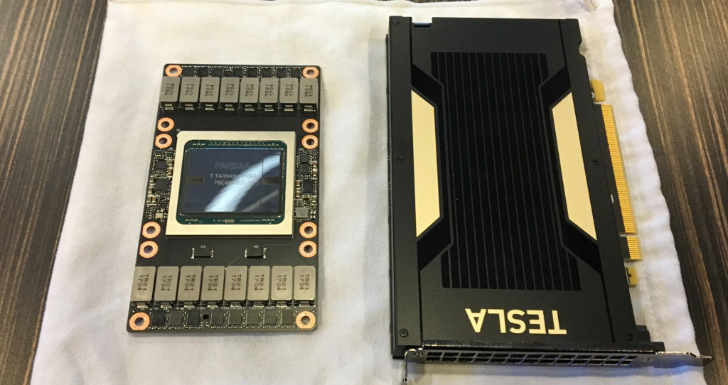
The right card is a 150w full Volta core enabled Tesla... albeit greatly reduced clocks. SXM2 is 300w, full sized pcie 250w, and baby volta 150w.
The SXM2 cards are pretty nuts...
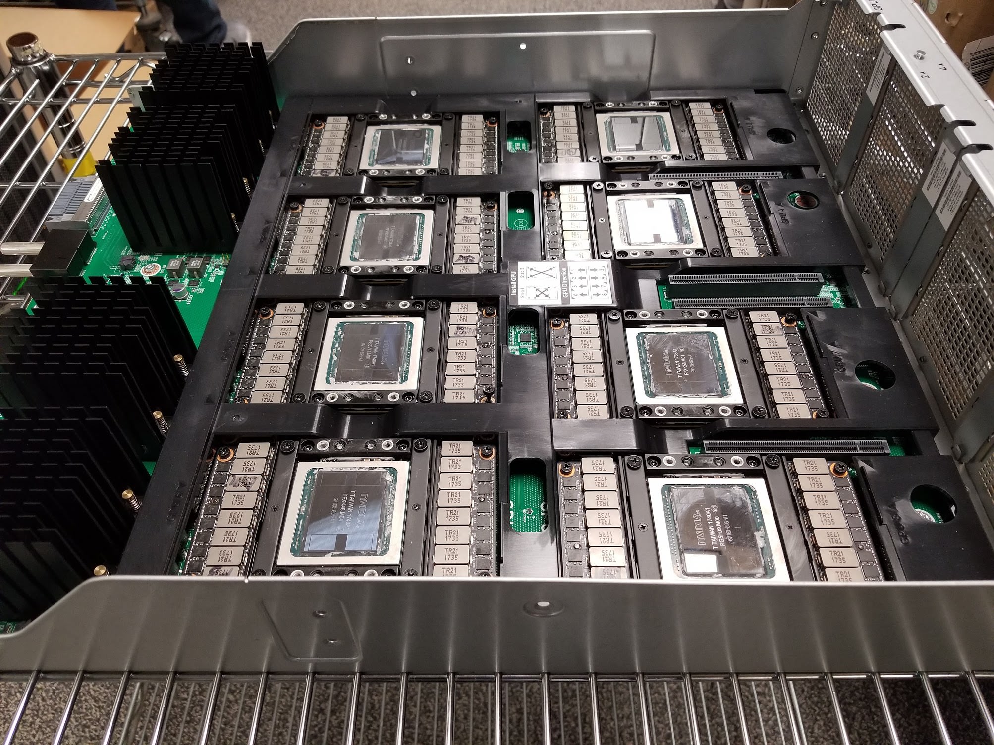
Had to go dig through my pictures, the baby v100 (150w variant) is not nvlink enabled, no gold finger, the big one can do 2 way, and the sxm2 can do 4/8/16 way. Most servers are 4 or 8 sxm2 though... only dgx2 supports 16 way...and costs what 400k.
My guess would be quadro or consumer volta/turning sample for testing gddr6.
Last edited: