- Joined
- Oct 9, 2007
- Messages
- 47,684 (7.42/day)
- Location
- Dublin, Ireland
| System Name | RBMK-1000 |
|---|---|
| Processor | AMD Ryzen 7 5700G |
| Motherboard | Gigabyte B550 AORUS Elite V2 |
| Cooling | DeepCool Gammax L240 V2 |
| Memory | 2x 16GB DDR4-3200 |
| Video Card(s) | Galax RTX 4070 Ti EX |
| Storage | Samsung 990 1TB |
| Display(s) | BenQ 1440p 60 Hz 27-inch |
| Case | Corsair Carbide 100R |
| Audio Device(s) | ASUS SupremeFX S1220A |
| Power Supply | Cooler Master MWE Gold 650W |
| Mouse | ASUS ROG Strix Impact |
| Keyboard | Gamdias Hermes E2 |
| Software | Windows 11 Pro |
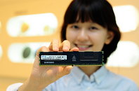
Samsung Electronics, Ltd. announced today that it has started mass producing the industry's first 64 gigabyte (GB), double data rate-4 (DDR4), registered dual Inline memory modules (RDIMMs) that use three dimensional (3D) "through silicon via" (TSV) package technology. The new high-density, high-performance module will play a key role in supporting the continued proliferation of enterprise servers and cloud-based applications, as well as further diversification of data center solutions.
The new RDIMMs include 36 DDR4 DRAM chips, each of which consists of four 4-gigabit (Gb) DDR4 DRAM dies. The low-power chips are manufactured using Samsung's most advanced 20-nanometer (nm) class* process technology and 3D TSV package technology.
"Samsung is reinforcing its competitive edge in the DRAM market with its new state-of-the-art solution using its 3D TSV technology, while driving growth in the global DRAM market," said Jeeho Baek, vice president, memory marketing, Samsung Electronics. "By introducing highly energy-efficient DDR4 modules assembled with 3D TSV, we're taking a big step ahead of the mainstream DDR4 market, which should dramatically expand with the expected introduction of next-generation CPUs in the second half of this year."
Samsung's volume production of 3D TSV modules marks a new milestone in the history of memory technology, following the company's initial production of 3D Vertical NAND (V-NAND) flash memory last year. While 3D V-NAND technology embraces high-rise vertical structures of cell arrays inside a monolithic die, 3D TSV is an innovative packaging technology that vertically interconnects stacked dies. With its introduction of the new TSV modules, Samsung has further strengthened its technological leadership in the "3D memory" era.
To build a 3D TSV DRAM package, the DDR4 dies are ground down as thin as a few dozen micrometers, then pierced to contain hundreds of fine holes. They are vertically connected through electrodes that are passed through the holes. As a result, the new 64GB TSV module performs twice as fast as a 64GB module that uses wire bonding packaging, while consuming approximately half the power.
In the future, Samsung believes that it will be able to stack more than four DDR4 dies using its 3D TSV technology, to create even higher density DRAM modules. This will accelerate expansion of the premium memory market, in line with an acceleration of the transition from DDR3 to DDR4 throughout the server market.
Samsung has worked on improving 3D TSV technology since it developed 40nm-class* 8GB DRAM RDIMMs in 2010 and 30nm-class* 32GB DRAM RDIMMs in 2011 using 3D TSV. This year, Samsung started operating a new manufacturing system dedicated to TSV packaging, for mass producing the new server modules.
According to a research report from Gartner, the global DRAM market is expected to reach U.S. $38.6 billion and 29.8 billion units (1Gb equivalent) by year-end. Gartner also predicted that the server market will account for more than 20 percent of DRAM production this year with approximately 6.7 billion units (1Gb equivalent).
View at TechPowerUp Main Site
The new RDIMMs include 36 DDR4 DRAM chips, each of which consists of four 4-gigabit (Gb) DDR4 DRAM dies. The low-power chips are manufactured using Samsung's most advanced 20-nanometer (nm) class* process technology and 3D TSV package technology.

"Samsung is reinforcing its competitive edge in the DRAM market with its new state-of-the-art solution using its 3D TSV technology, while driving growth in the global DRAM market," said Jeeho Baek, vice president, memory marketing, Samsung Electronics. "By introducing highly energy-efficient DDR4 modules assembled with 3D TSV, we're taking a big step ahead of the mainstream DDR4 market, which should dramatically expand with the expected introduction of next-generation CPUs in the second half of this year."
Samsung's volume production of 3D TSV modules marks a new milestone in the history of memory technology, following the company's initial production of 3D Vertical NAND (V-NAND) flash memory last year. While 3D V-NAND technology embraces high-rise vertical structures of cell arrays inside a monolithic die, 3D TSV is an innovative packaging technology that vertically interconnects stacked dies. With its introduction of the new TSV modules, Samsung has further strengthened its technological leadership in the "3D memory" era.
To build a 3D TSV DRAM package, the DDR4 dies are ground down as thin as a few dozen micrometers, then pierced to contain hundreds of fine holes. They are vertically connected through electrodes that are passed through the holes. As a result, the new 64GB TSV module performs twice as fast as a 64GB module that uses wire bonding packaging, while consuming approximately half the power.
In the future, Samsung believes that it will be able to stack more than four DDR4 dies using its 3D TSV technology, to create even higher density DRAM modules. This will accelerate expansion of the premium memory market, in line with an acceleration of the transition from DDR3 to DDR4 throughout the server market.
Samsung has worked on improving 3D TSV technology since it developed 40nm-class* 8GB DRAM RDIMMs in 2010 and 30nm-class* 32GB DRAM RDIMMs in 2011 using 3D TSV. This year, Samsung started operating a new manufacturing system dedicated to TSV packaging, for mass producing the new server modules.
According to a research report from Gartner, the global DRAM market is expected to reach U.S. $38.6 billion and 29.8 billion units (1Gb equivalent) by year-end. Gartner also predicted that the server market will account for more than 20 percent of DRAM production this year with approximately 6.7 billion units (1Gb equivalent).
View at TechPowerUp Main Site

")
")