- Joined
- Oct 9, 2007
- Messages
- 47,774 (7.41/day)
- Location
- Dublin, Ireland
| System Name | RBMK-1000 |
|---|---|
| Processor | AMD Ryzen 7 5700G |
| Motherboard | Gigabyte B550 AORUS Elite V2 |
| Cooling | DeepCool Gammax L240 V2 |
| Memory | 2x 16GB DDR4-3200 |
| Video Card(s) | Galax RTX 4070 Ti EX |
| Storage | Samsung 990 1TB |
| Display(s) | BenQ 1440p 60 Hz 27-inch |
| Case | Corsair Carbide 100R |
| Audio Device(s) | ASUS SupremeFX S1220A |
| Power Supply | Cooler Master MWE Gold 650W |
| Mouse | ASUS ROG Strix Impact |
| Keyboard | Gamdias Hermes E2 |
| Software | Windows 11 Pro |
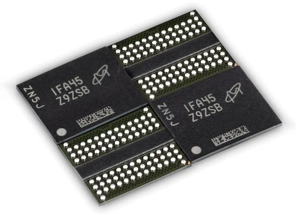
Samsung Electronics, the world leader in advanced memory technology, today announced that it has begun mass producing the industry's smallest, 14-nanometer (nm), DRAM based on extreme ultraviolet (EUV) technology. Following the company's shipment of the industry-first EUV DRAM in March of last year, Samsung has increased the number of EUV layers to five to deliver today's finest, most advanced DRAM process for its DDR5 solutions.
"We have led the DRAM market for nearly three decades by pioneering key patterning technology innovations," said Jooyoung Lee, Senior Vice President and Head of DRAM Product & Technology at Samsung Electronics. "Today, Samsung is setting another technology milestone with multi-layer EUV that has enabled extreme miniaturization at 14 nm—a feat not possible with the conventional argon fluoride (ArF) process. Building on this advancement, we will continue to provide the most differentiated memory solutions by fully addressing the need for greater performance and capacity in the data-driven world of 5G, AI and the metaverse."
As DRAM continues to scale down the 10 nm-range, EUV technology becomes increasingly important to improve patterning accuracy for higher performance and greater yields. By applying five EUV layers to its 14 nm DRAM, Samsung has achieved the highest bit density while enhancing the overall wafer productivity by approximately 20%. Additionally, the 14 nm process can help bring down power consumption by nearly 20% compared to the previous-generation DRAM node.
Leveraging the latest DDR5 standard, Samsung's 14 nm DRAM will help unlock unprecedented speeds of up to 7.2 gigabits per second (Gbps), which is more than twice the DDR4 speed of up to 3.2 Gbps.
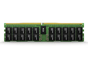
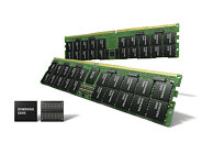
Samsung plans to expand its 14 nm DDR5 portfolio to support data center, supercomputer and enterprise server applications. Also, Samsung expects to grow its 14 nm DRAM chip density to 24Gb in better meeting the rapidly-growing data demands of global IT systems.
View at TechPowerUp Main Site
"We have led the DRAM market for nearly three decades by pioneering key patterning technology innovations," said Jooyoung Lee, Senior Vice President and Head of DRAM Product & Technology at Samsung Electronics. "Today, Samsung is setting another technology milestone with multi-layer EUV that has enabled extreme miniaturization at 14 nm—a feat not possible with the conventional argon fluoride (ArF) process. Building on this advancement, we will continue to provide the most differentiated memory solutions by fully addressing the need for greater performance and capacity in the data-driven world of 5G, AI and the metaverse."


As DRAM continues to scale down the 10 nm-range, EUV technology becomes increasingly important to improve patterning accuracy for higher performance and greater yields. By applying five EUV layers to its 14 nm DRAM, Samsung has achieved the highest bit density while enhancing the overall wafer productivity by approximately 20%. Additionally, the 14 nm process can help bring down power consumption by nearly 20% compared to the previous-generation DRAM node.
Leveraging the latest DDR5 standard, Samsung's 14 nm DRAM will help unlock unprecedented speeds of up to 7.2 gigabits per second (Gbps), which is more than twice the DDR4 speed of up to 3.2 Gbps.
Samsung plans to expand its 14 nm DDR5 portfolio to support data center, supercomputer and enterprise server applications. Also, Samsung expects to grow its 14 nm DRAM chip density to 24Gb in better meeting the rapidly-growing data demands of global IT systems.
View at TechPowerUp Main Site


")