• Welcome to TechPowerUp Forums, Guest! Please check out our forum guidelines for info related to our community.

SanDisk Develops HBM Killer: High-Bandwidth Flash (HBF) Allows 4 TB of VRAM for AI GPUs

AleksandarK

News Editor
Staff member
Joined
Aug 19, 2017
Messages
2,999 (1.07/day)
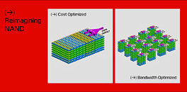
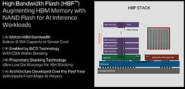
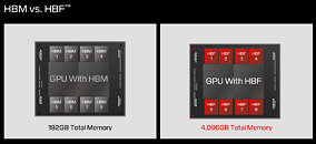
During its first post-Western Digital spinoff investor day, SanDisk showed something it has been working on to tackle the AI sector. High-bandwidth flash (HBF) is a new memory architecture that combines 3D NAND flash storage with bandwidth capabilities comparable to high-bandwidth memory (HBM). The HBF design stacks 16 3D NAND BiCS8 dies using through-silicon vias, with a logic layer enabling parallel access to memory sub-arrays. This configuration achieves 8 to 16 times greater capacity per stack than current HBM implementations. A system using eight HBF stacks can provide 4 TB of VRAM to store large AI models like GPT-4 directly on GPU hardware. The architecture breaks from conventional NAND design by implementing independently accessible memory sub-arrays, moving beyond traditional multi-plane approaches. While HBF surpasses HBM's capacity specifications, it maintains higher latency than DRAM, limiting its application to specific workloads.

SanDisk has not disclosed its solution for NAND's inherent write endurance limitations, though using pSLC NAND makes it possible to balance durability and cost. The bandwidth of HBF is also unknown, as the company hasn't put out details yet. SanDisk Memory Technology Chief Alper Ilkbahar confirmed the technology targets read-intensive AI inference tasks rather than latency-sensitive applications. The company is developing HBF as an open standard, incorporating mechanical and electrical interfaces similar to HBM to simplify integration. Some challenges remain, including NAND's block-level addressing limitations and writing endurance constraints. While these factors make HBF unsuitable for gaming applications, the technology's high capacity and throughput characteristics align with AI model storage and inference requirements. SanDisk has announced plans for three generations of HBF development, indicating a long-term commitment to the technology.
View at TechPowerUp Main Site | Source
 
Some challenges remain, including NAND's block-level addressing limitations and writing endurance constraints.
It's actually page-level reading/writing and block-level erasing, where a page is 4 ki-bi-bytes and a block is a few megabytes. However, the architecture of HBF seems to be a lot different, and the page size may also be smaller (or larger) if Sandisk thinks it's better for the purpose.
Even DRAM is far from being byte-addressable; the smallest unit of transfer is 64 bytes in DDR, 32 bytes in HBM3, and I think it's the same in HBM3E.
It isn't just the granularity of transfer. DRAM has unlimited endurance; this, on the other hand, is unlikely to be much better than SLC.
Soooo...what ya'll are saying is that there won't be any 4TB, $25K GPU's for da gamrz to drool over, at least not for a while anyways ?

Aw so sad :D


n.O.t.....
 
Last edited:
I assume it is mostly meant for Large AI models, which require quite a lot of vram to run. Performance as memory will not be great but if it's performant enough, with the dram on top, it may very well be good enough.
If so good development to bring costs down for these.
 
Previous attempts to use non-RAM as RAM failed.
The most famous one was Intel/Micron Optane/3D XPoint.
It doesn't seem that this one will do any better.
 
Soooo...what ya'll are saying is that there won't be any 4TB, $25K GPU's for us gamrz to drool over, at least not for a while anyways ?

Aw so sad :D


n.O.t.....
The trend is obviously towards 8GB, $25K GPUs, but the frog tastes best if cooked slowly.

Correct me if I'm wrong... but AI models would rapidly degrade NAND storage, making it impractical for long-term use, since NAND ( when used as VRAM) requires continuous high-frequency read and write operations.
The models would only be updated occasionally, that's the idea, so writing wouldn't be much of a problem. But limited read endurance is also sometimes hinted at. I don't know how much research has been done around read degradation, and whether it's relevant. Anyway, processing needs RAM too, a couple hundred MB of static RAM cache can't suffice for that, so inevitably some HBM will be part of the system too.
 
This HBF looks 'useful', but not on its own.
Inb4 tiered memory standards for Compute/Graphics?

Top: L1-3 caches
Upper: HBM
Lower: HBF
Bottom: NAND

Stack it 'till it's cheap :laugh:
 
Yeah, no. NAND flash is not RAM, it is designed for entirely different usage patterns, and the notion that it could be used as a replacement for RAM is nonsensical. Considering GPUs already have effectively direct access to storage via APIs like DirectStorage, I see no use-case for this technology.
 
Correct me if I'm wrong... but AI models would rapidly degrade NAND storage, making it impractical for long-term use, since NAND ( when used as VRAM) requires continuous high-frequency read and write operations.

It depends, is the AI model being constantly loaded or can it simply stay in memory?

If they are using flash here it may be non-volatile which could make it quite flexible.
 
It depends, is the AI model being constantly loaded or can it simply stay in memory?

If they are using flash here it may be non-volatile which could make it quite flexible.
Looking towards 'applications' in a given 'product',
maybe, parts of a Model can better utilize different kinds of storage?

I'm thinking:
"Working memory" Cache, HBM, RAM.
"Short-Term Memory" HBF, XLflash, phase-change memory, massively parallelized (p)SLC NAND.
"Long-Term Memory" TLC and QLC NAND.
"Archival Memory" HDDs and Magnetic Tape.
 
Last edited:
Correct me if I'm wrong... but AI models would rapidly degrade NAND storage, making it impractical for long-term use, since NAND ( when used as VRAM) requires continuous high-frequency read and write operations.

There are two cases: Training ( write ops ) and Inference ( read ops, where they intend to use HBF ). Its overall indurance depends on Terrabyte Written ( TBW ).

Also, that new technology could affect progress of CXL Memory Expanders ( very expensive stuff right now ). 4TB inside of a GPU is a lot of memory for processing!
 
It depends, is the AI model being constantly loaded or can it simply stay in memory?

If they are using flash here it may be non-volatile which could make it quite flexible.
Non-volatility means little, or nothing, in this kind of applications. The processors will crunch vectors and matrices without interruption until they're too old and can't make enough money anymore. (Well, low power and sleep states probably exist too, since all processors can't be fully loaded all of the time.)

Also, that new technology could affect progress of CXL Memory Expanders ( very expensive stuff right now ).
I don't see a close connection. CXL is PCIe, which is up to 16 lanes of Gen 6 (maybe soon in AI datacenters) or Gen 7 (a few years out). That's infinitely slower than several stacks of on-package HBM/HBF optimised for maximum bandwidth and maximum cost.
 
Non-volatility means little, or nothing, in this kind of applications. The processors will crunch vectors and matrices without interruption until they're too old and can't make enough money anymore. (Well, low power and sleep states probably exist too, since all processors can't be fully loaded all of the time.)

Non-volatile memory yields power and cost savings. There are dozens of articles on the topic: https://www.embedded.com/the-benefit-of-non-volatile-memory-nvm-for-edge-ai/


It allows you to take fetches that would otherwise be to main system memory or mass storage and put them right on the chip. This lowers latency and power consumption. In addition, flash doesn't needed to be constantly refreshed when not actively in use so you can very aggressively power tune it. This is simply not possible with volatile memory that needs to be refreshed to maintain data.

I believe LabRat 891 put it perfectly, it makes sense as another layer in the memory subsystem designed to hold a specific set of data and the overall workload will see a very nice benefit as a result.
 
It can operate at what bandwidth dear sir?Bandwidth is in its name after all.
1bit per second, arbitrary value.
 
If it isn't readily serviceable and replaceable the NAND seems like a serious e-waste concern for the rest of the hardware if the NAND degrades too quickly. It might be acceptable for AI depending on longevity, but probably not so much otherwise.
 
Non-volatile memory yields power and cost savings. There are dozens of articles on the topic: https://www.embedded.com/the-benefit-of-non-volatile-memory-nvm-for-edge-ai/


It allows you to take fetches that would otherwise be to main system memory or mass storage and put them right on the chip. This lowers latency and power consumption. In addition, flash doesn't needed to be constantly refreshed when not actively in use so you can very aggressively power tune it. This is simply not possible with volatile memory that needs to be refreshed to maintain data.

I believe LabRat 891 put it perfectly, it makes sense as another layer in the memory subsystem designed to hold a specific set of data and the overall workload will see a very nice benefit as a result.
I don't disagree, NAND does have some advantages, but non-volatility by itself is not important unless and until power goes out. A theoretical volatile NAND with extremely low idle power (similar to SRAM) would do this job just as well, that's my point.

Anther reminder it was dumb to kill off xpoint, it would have been as in demand as hbm for the last 2 years
We can't be sure it's dead. The development continues somewhere deep under the ground and will continue until all patents expire. TI (or whoever) may succeed in developing a method to expand those 4 layers to 100+ ... but it's not a given.

It can operate at what bandwidth dear sir?Bandwidth is in its name after all.
1bit per second, arbitrary value.
HBM sends the data around at about 6400 MT/s, and NAND does it at 3200 MT/s. So, as a quick estimate, half of HBM's bandwidth would be possible with the technology we already have.
 
SanDisk Develops HBM Killer: High-Bandwidth Flash (HBF)
Wait, what?...
While HBF surpasses HBM's capacity specifications, it maintains higher latency than DRAM, limiting its application to specific workloads.
So this is NAND... HBM is DRAM...

NOT an HBM killer. That was a very click-bait headline. Come on peeps, TPU is better than that crap..
 
Wait, what?...

So this is NAND... HBM is DRAM...

NOT an HBM killer. That was a very click-bait headline. Come on peeps, TPU is better than that crap..
For AI workloads its HBM killer(despite being not the same tech fundamentally). Imagine you load an entire model on a single GPU. You don't need top-tier low-latency.
 
If they can somehow do this on a M.2 attached to a GPU and get similar results it would be great. If it's just replacing volatile VRAM with NAND and questionable endurance concerns maybe not as exciting. From a business standpoint it could still make a lot of sense though if the economics of it make enough sense in terms of profitability.
 
For AI workloads its HBM killer(despite being not the same tech fundamentally). Imagine you load an entire model on a single GPU. You don't need top-tier low-latency.
While that's a fair point, I was referring to the durability factor. NAND wears out, and under these kinds of load, would wear out swiftly. This is fact and can not be argued. DRAM does not wear out.

That was my point. For that reason alone, HBF is NOT an HBM killer. Until we have a major break-through in NAND flash durability it will not change. All Sandisk has done is create mildly and temporarily useful E-waste.
 
They're already saying it's for AI inference, i.e. mostly read-centric workloads where most of the bandwidth utilization is reading model weights (in the hundreds of gigabytes to few terabytes range). Nothing prohibits hardware manufacturers from putting VRAM or HBM alongside the HBF for memory content that needs to be frequently modified (mainly the key-value cache during token generation).
 

Attachments

  • 1739537039325.png
    1739537039325.png
    111.6 KB · Views: 53
  • 1739537164662.png
    1739537164662.png
    150.6 KB · Views: 27
They're already saying it's for AI inference, i.e. mostly read-centric workloads where most of the bandwidth utilization is reading model weights (in the hundreds of gigabytes to few terabytes range).
While that is a reasonable point, NAND flash simply doesn't have the durability to be useful long term in such a way.
Nothing prohibits hardware manufacturers from putting VRAM or HBM alongside the HBF for memory content that needs to be frequently modified (mainly the key-value cache during token generation).
Another reasonable point, however, that was not the claim made in the above article.
 
Back
Top